-
Hot

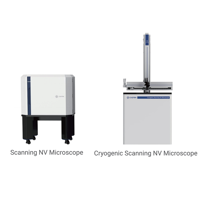
Scanning NV Microscope for Laboratory Material Analysis
The Scanning NV Microscope is a quantum precision measurement instrument that combines optically detected magnetic resonance (ODMR) of diamond nitrogen-vacancy centers with scanning probe technique. It is applicable to research in spintronics, multiferroics, 2D magnetic materials, superconductors, and more.
Send Email Details -
Hot
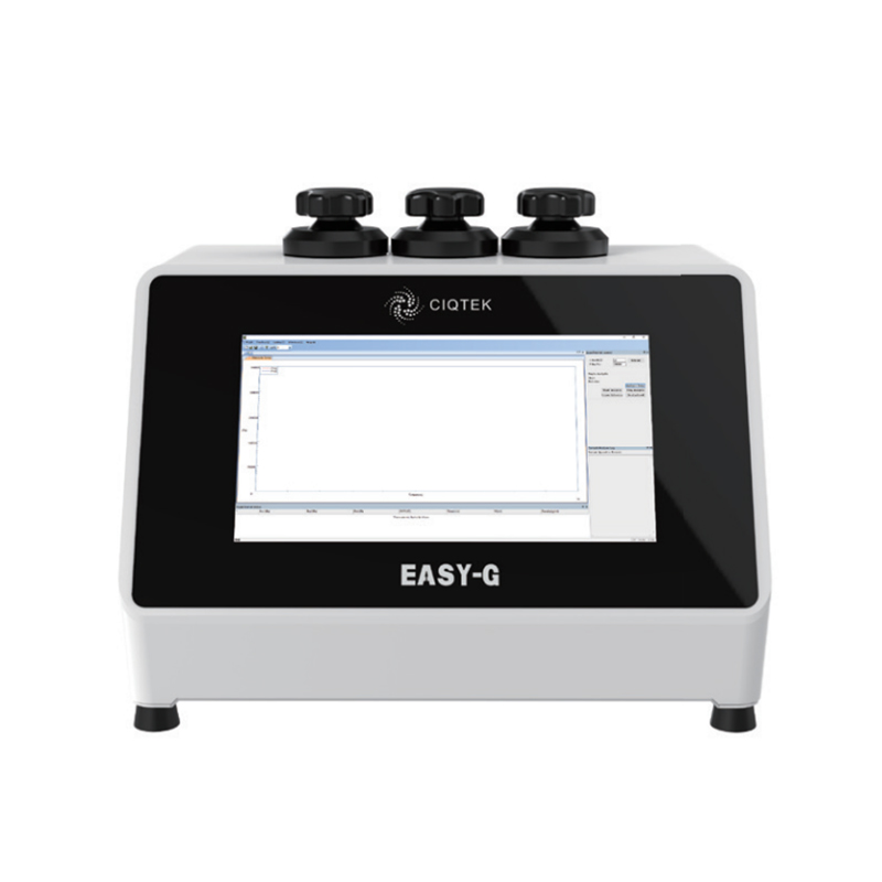
EASY-G 1310M Gas Pycnometer for Laboratory Material Analysis
The EASY-G 1310M gas pycnometer delivers ±0.02% accuracy and ±0.01% repeatability in true density measurement. Features 3-sample chambers, 13.3" embedded computer, integrated pipeline system, and dual-pressure modes (negative/positive). Ideal for powders, batteries, coal, soil, and food, with rapid industrial QC capabilities.
EASY-G 1310M Gas Pycnometer for Laboratory Material Analysis High-Precision True Density Analyzer with Multi-Sample Chamber True density analyzerSend Email Details -
Hot
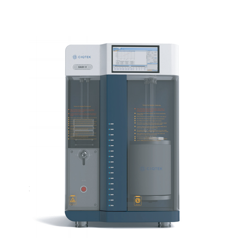
Specific Surface And Porosimetry Analyzer EASY-V
The EASY-V series products adopt the static volume method for specific surface testing and pore size analysis. They have been delivered to multiple universities and research institutions worldwide and are well-received by users. The series is fully automated, with a user-friendly and easy-to-learn interface. The technology has obtained several international certifications and reaches world-class levels. Its high cost-performance effectively ensures user investment interests, and flexible product configuration meets diverse user needs.
Specific Surface And Porosimetry Analyzer EASY-V Specific surface area analyzer Pore size distribution measurementSend Email Details -
Hot
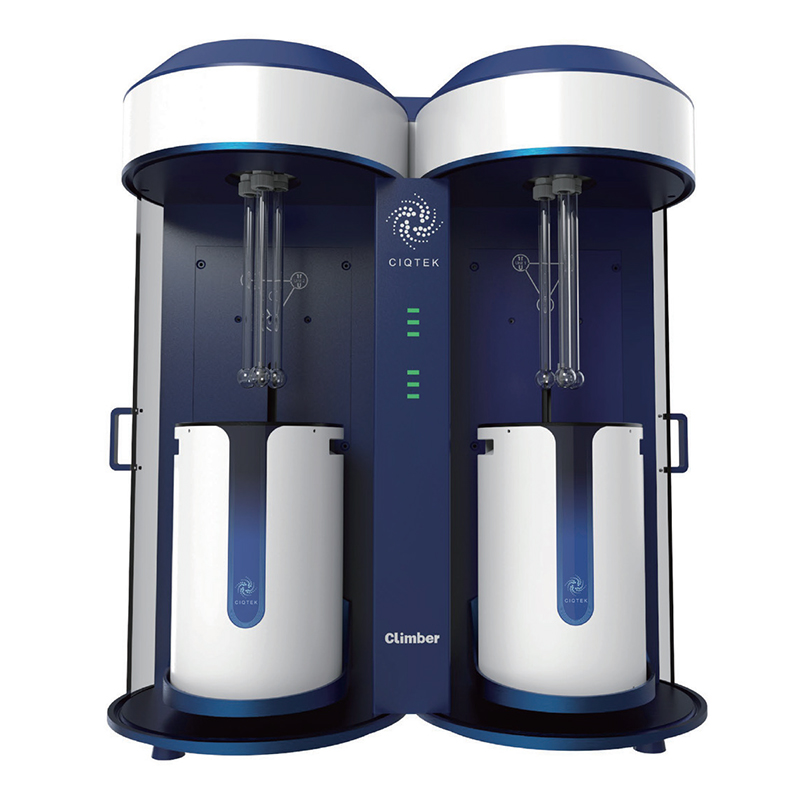
Climber Series Specific Surface And Porosimetry Analyzer
The Climber Series Specific Surface Area and Pore Size Analyzers are designed for fast, accurate, and stable testing, supporting up to 6 samples analyzed simultaneously. Key capabilities include: Testing specific surface area and pore size
Climber Series Specific Surface And Porosimetry Analyzer Dual-module independent control analyzer Battery material analysis equipmentSend Email Details -
Hot
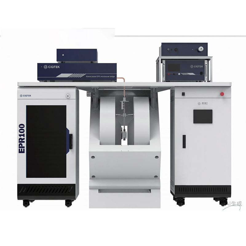
EPR Series Spectrometers And Resonators
The EPR Series combines X-band CW (EPR300) and pulsed (EPR100) spectrometers with advanced resonators (PW-4201-DR, High-Q, Dual-Mode). EPR100 delivers 200mW CW/pulsed power, 500W SSPA, and 4ns timing resolution; EPR300 offers 10,000:1 SNR and Q-band extension. Resonators feature 400MHz FWHM (PW-4201-DR), ≥18,000 Q-factor (High-Q), and dual-mode frequencies. Ideal for materials science, chemistry, and quantum research with automated workflows and multi-nucleus detection.
Send Email Details -
Hot
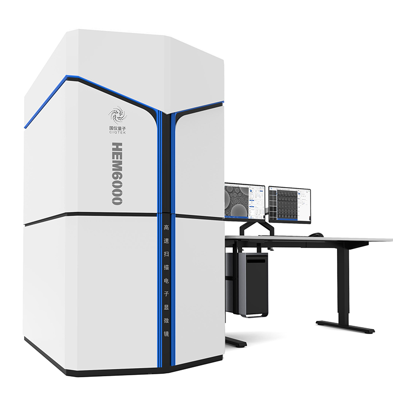
HEM6000 High-Speed Scanning Electron Microscope
High - speed Scanning Driver Dwell time: 10 ns/pixel; Maximum acquisition speed: 2×100M pixel/s Electron Filtering System SE/BSE signals can be freely switched, and the mixing ratio of signals is adjustable. All - electrostatic High - speed
HEM6000 High-Speed Scanning Electron Microscope Industrial SEM for Semiconductor Inspection Low-Voltage High-Resolution SEMSend Email Details -
Hot
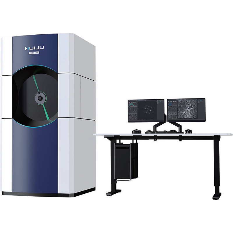
Field Emission Transmission Electron Microscope
TH120 120kV Field Emission TEM integrates Schottky emission gun, parallel/convergent beam auto - switch, symmetric obj. lens. Features high - res CMOS cam, 4 - axis stage, integrated software. Divided workspaces cut interference; automated workflows boost efficiency; upgrade - ready design suits diverse R&D needs.
Field Emission Transmission ElectronMicroscope 120kV Field Emission Transmission Microscope TH120 Advanced Lab Imaging SolutionSend Email Details -
Hot
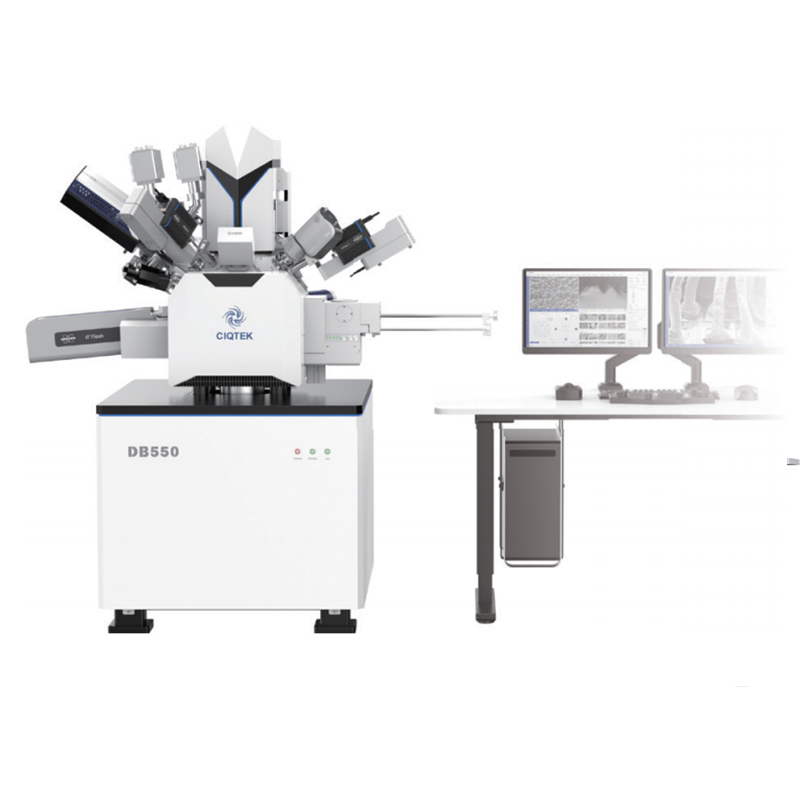
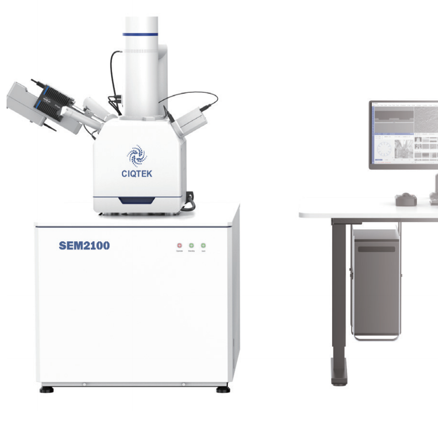
DB550 Ga+ Focused Ion Beam Field Emission Scanning Electron Microscope
The DB550 integrates a Ga+ Focused Ion Beam (FIB) column with a Field Emission SEM, featuring "Super Tunnel" electron optics (low aberration, magnetic-free lens), 3nm@30kV ion resolution, and 0.9nm@15kV SEM resolution. It includes a nanomanipulator (≤10nm precision), gas injection system (single GIS, ±0.1°C temp control), and 8-inch compatible loadlock. Ideal for nano-fabrication, semiconductor failure analysis, and materials characterization with automated workflows and expandable detectors (EDS/EBSD/STEM).
DB550 Ga+ Focused Ion Beam Field Emission Scanning Electron Microscope Integrated FIB-SEM workstation Super Tunnel electron opticsSend Email Details -
Hot
SEM-X Series Ultra-High Resolution Schottky Field Emission Scanning Electron Microscope
The SEM-X Series delivers breakthrough resolution (0.6nm@15kV, 1.2nm@1kV) with low-voltage imaging, minimizing sample damage. It integrates "Super-Tunnel" electron optics, electrostatic-electromagnetic compound lenses, and dual-beam deceleration technology for aberration-free performance. Features include low-vacuum mode (10-180Pa), 8-inch compatible loadlock, and multi-detector systems (UD-SE/BSE, LD, LVD) for versatile analysis. Ideal for semiconductor, materials science, and life sciences, offering automation and expandability forsearch applications.
Send Email Details -
Hot
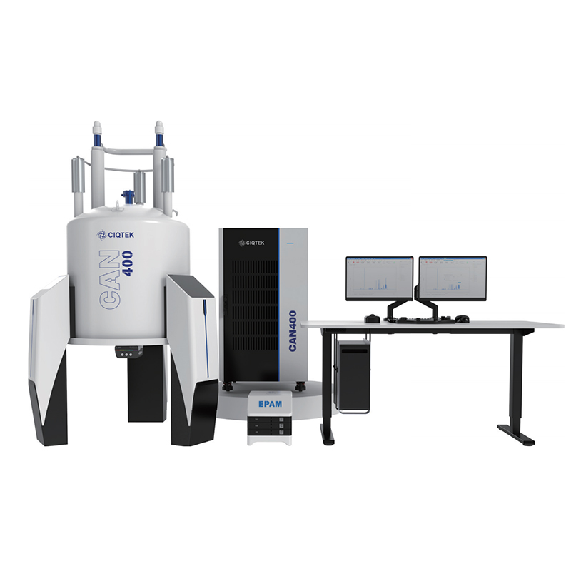
CAN400 Intelligent Liquid-State NMR Spectrometer
The CAN400 features a 9.39 Tesla 400 MHz superconducting magnet with 54 mm bore for ultra-high homogeneity. Its distributed console supports 2–8 RF channels, 4 ns timing resolution, and software-controlled power management. Equipped with a 72-slot auto sample changer, intelligent touchscreen, and multi-nucleus probe, it enables rapid, automated analysis. Ideal for chemistry, energy, and pharma, it offers in-situ experiments, remote access, and versatile applications from battery research to drug screening.
CAN400 Intelligent Liquid-State NMR Spectrometer 400 MHz superconducting magnet Distributed console NMRSend Email Details -
Hot
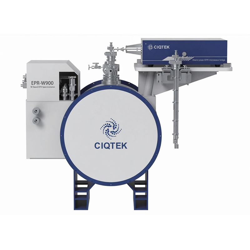
W900 W-Band High-Frequency EPR Spectrometer
The W900 operates at 94 GHz for superior spectral and orientational resolution in disordered systems. It features a W-band microwave bridge (93.5–94.5 GHz, 30 mW CW/2 W pulse), a 6-free superconducting magnet with ±1000 Gauss scan coils, and a high-Q resonator (≥4000 Q-value, 93.7–94.4 GHz). Paired with EPR ProCT software for automated CW/pulsed experiments (DEER/EDNMR/ENDOR), it enables precise quantum material and radical analysis.
Send Email Details