

SEM-X Series Ultra-High Resolution Schottky Field Emission Scanning Electron Microscope
The SEM-X Series delivers breakthrough resolution (0.6nm@15kV, 1.2nm@1kV) with low-voltage imaging, minimizing sample damage. It integrates "Super-Tunnel" electron optics, electrostatic-electromagnetic compound lenses, and dual-beam deceleration technology for aberration-free performance. Features include low-vacuum mode (10-180Pa), 8-inch compatible loadlock, and multi-detector systems (UD-SE/BSE, LD, LVD) for versatile analysis. Ideal for semiconductor, materials science, and life sciences, offering automation and expandability forsearch applications.
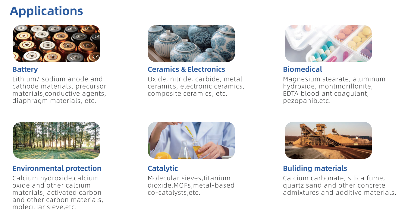
SEM-X Series Ultra-High Resolution Schottky Field Emission Scanning Electron Microscope Applications and Related Testing Solutions
SEM-X Series Ultra-High Resolution Schottky Field Emission Scanning Electron Microscope supports precision inspection and analysis tasks that require clear imaging, stable test conditions, and dependable laboratory or production quality control.
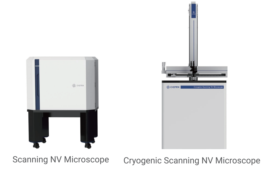
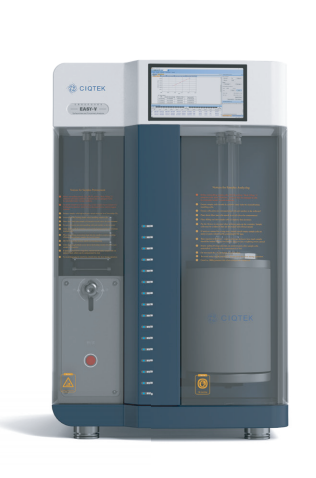
Related Products: Scanning NV Microscope | EASY-G 1310M Gas Pycnometer | Specific Surface & Porosimetry Analyzer EASY-V
Product Description
The SEM-X Series Ultra-High Resolution Schottky Field Emission Scanning Electron Microscope redefines nano-imaging by merging ultrahigh resolution, low-voltage sensitivity, and advanced analytical capabilities. Built on a legacy of flagship models (SEM4000X/Pro, SEM5000X/Pro, SEM3200/3300), it integrates cutting-edge technologies to address diverse research and industrial needs, from semiconductor failure analysis to nanomaterials characterization.
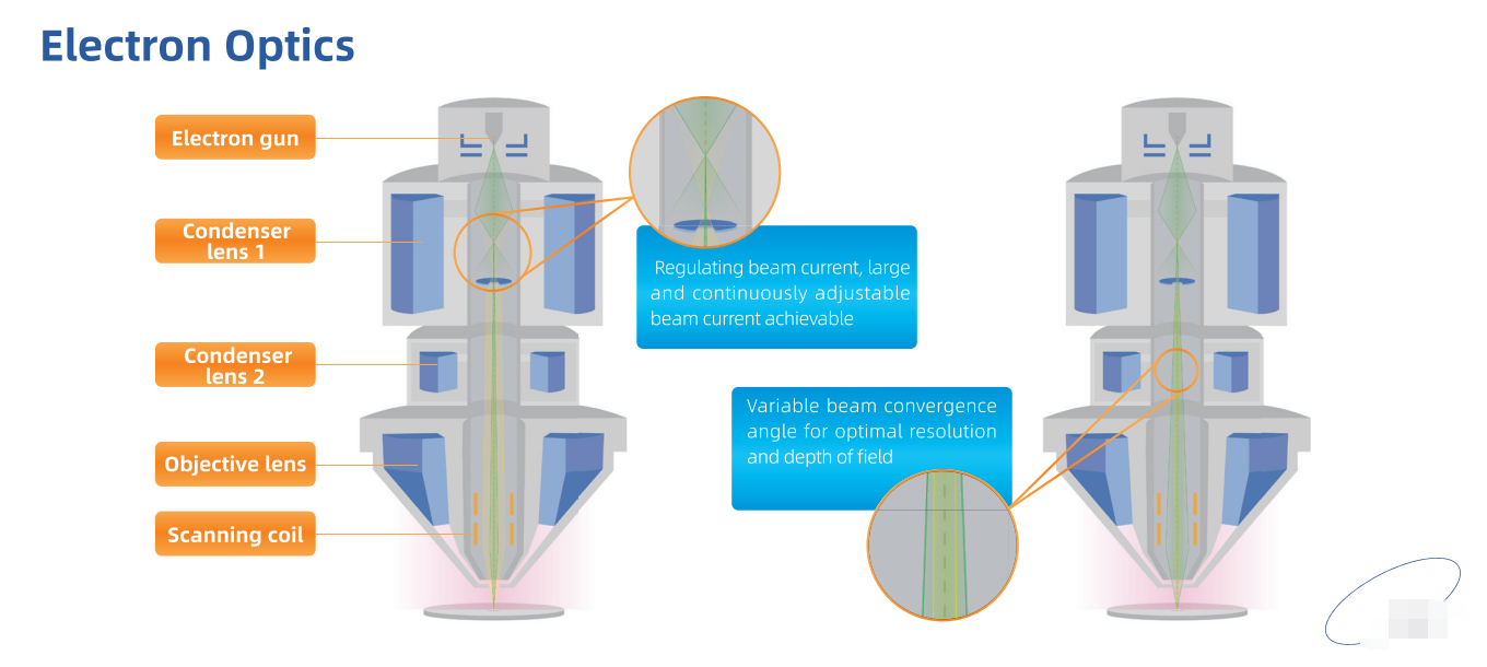
Core Technological Architecture
The SEM-X Series is engineered around five pillars of innovation:
Schottky Field Emission Electron Gun: A high-brightness, long-life gun generates a stable electron beam with adjustable current (1pA–65nA), enabling precise imaging of delicate samples. Pre-aligned filaments (SEM3200/3300) ensure consistent performance, while dual-anode structures (SEM3200) boost low-voltage resolution by 10% and signal-to-noise ratio by 30%.
"Super Optics: This proprietary technology eliminates beam crossovers, reducing spatial charging effects and lens aberrations. Combined with electrostatic-electromagnetic compound objective lenses (SEM5000Pro/5000X), it achieves 0.6nm@15kV resolution (SEM5000X) and 1.2nm@1kV (SEM5000Pro), surpassing traditional tungsten filament SEM limits (SEM3300 breaks 2.5nm@15kV).
Dual-Beam Deceleration Technology: Integrates in-lens beam deceleration (minimizing electron energy loss) and specimen stage tandem deceleration (enhancing signal capture). This reduces landing voltage while maintaining resolution, critical for non-conductive samples (e.g., polymers, biological tissues).
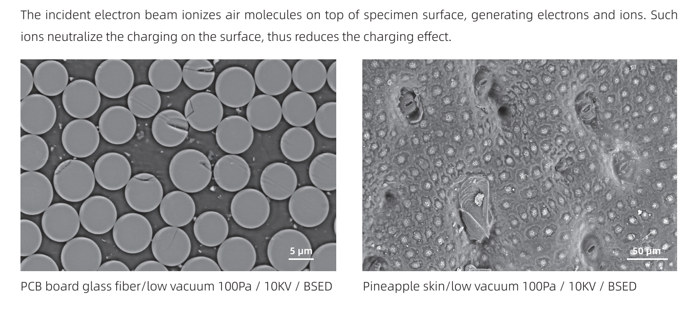
Low-Vacuum Mode: Operates at 10–180Pa without pressure-limiting apertures, using a specially designed objective lens vacuum chamber to achieve 1.5nm@30kV resolution. Gas ionization neutralizes surface charging (e.g., PCB boards, pineapple skin), enabling imaging of poorly conductive materials (SEM4000Pro).
Multi-Detector System: Includes in-column UD-SE/BSE detectors (high resolution), chamber-mounted LD detectors (stereoscopic imaging), low-vacuum LVD detectors (photon capture), and optional STEM/EDS/EBSDrystallographic analysis.
Key Components & Performance Specifications
The SEM-X Series features modular components optimized for flexibility:
Component | Specification |
|---|---|
Electron Gun | Schottky field emission (high brightness); dual-anode option (SEM3200) for 10% resolution boost. |
Resolution | 0.6nm@15kV (SEM5000X), 1.2nm@1kV (SEM5000Pro), 1.9nm@1kV (SEM4000X), 2.5nm@15kV (SEM3300). |
Objective Lens | Electrostatic-electromagnetic compound lens (SEM5000Pro/5000X); chromatic aberration reduced 12%, spherical 20%, total 30% (SEM5000X). |
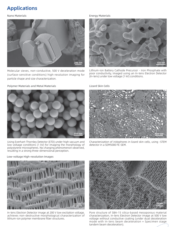
Beam Deceleration | Dual-mode: in-lens + specimen stage tandem (SEM5000X/3300); 500V deceleration for SBA-15 mesoporous materials. |
Vacuum System | Low-vacuum mode (10–180Pa, SEM4000Pro/5000Pro); fully automatic oil-free (SEM6000 series). |
Sample Stage | Mechanical eucentric stage (110mm X/Y travel, ±0.6μm repeatability); 8-inch (SEM4000Pro/5000Pro). |
Detectors | UD-SE/BSE, LD, LVD (low-vacuum), optional STEM/EDS/EBSD (SEM4000Pro), in-lens detector (SEM3300/5000Pro). |
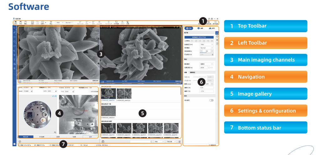
Automation | Auto-brightness/contrast, auto-focus, auto-stigmator, sample recognition (SEM4000X/6000 series). |
Applications Across Industries
Semiconductor: IC chip failure analysis (cross-section milling, TEM lamella prep), 7nm/5nm node inspection (SEM5000X/DB550-inspired FIB-SEM integration).
Materials Science: Nanostructure characterization (SBA-15 mesoporous materials, lithium battery cathodes), composite material analysis (carbon fibers, polymers).
Life Sciences: 3D neuron reconstruction (SEM6000-Bio), cell morphology studies (lizard skin iridophores),ductive tissue imaging (low-vacuum mode).
Industrial QC: PCB glass fiber inspection (100Pa low-vacuum), polymer fiber damage assessment (low-voltage mode), automotive part defect detection.
Advantages Over Conventional SEMs
Resolution & Speed: 5x faster imaging than conventional SEMs (2×100M pixel/s, 10ns/pixel dwell time, SEM6000), with sub-nanometer resolution.
Low-Voltage Sensitivity: Enables imaging of beam-sensitive samples (e.g., lithium batteries, biological tissues) without coating.
Versatility: Switches between high-vacuum (nanometer resolution) and low-vacuum (charging-prone samples) modes seamlessly.
Expandability: Supports optional accessories (nanomanipulators, gas injection systems, cryo-stages) for specialized applications.
SEO Keywords
Ultra-High Resolution Schottky Field Emission SEM
SEM-X Series Scanning Electron Microscope
Low-Voltage High-Resolution SEM
Super-Tunnel Electron Optics SEM
Dual-Beam Deceleration Technology SEM
0.6nm Resolution SEM
Low-Vacuum Mode SEM
8-Inch Compatible Loadlock SEM
Multi-Detector SEM for Materials Science
Automated Nano-Analysis SEM