

HEM6000 High-Speed Scanning Electron Microscope
High - speed Scanning Driver Dwell time: 10 ns/pixel; Maximum acquisition speed: 2×100M pixel/s Electron Filtering System SE/BSE signals can be freely switched, and the mixing ratio of signals is adjustable. All - electrostatic High - speed
HEM6000 High-Speed Scanning Electron Microscope Applications and Related Testing Solutions
HEM6000 High-Speed Scanning Electron Microscope supports precision inspection and analysis tasks that require clear imaging, stable test conditions, and dependable laboratory or production quality control.
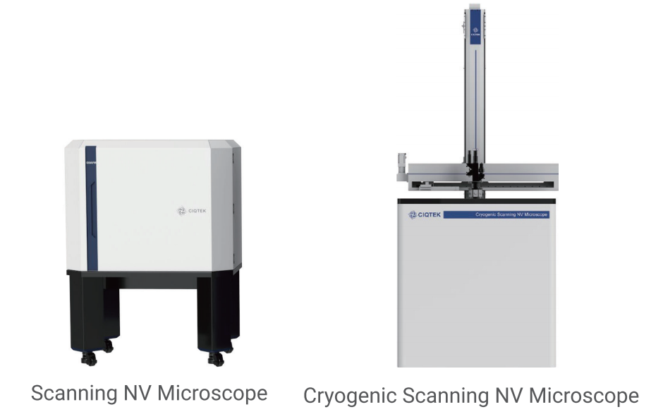
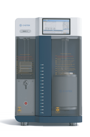
Related Products: Scanning NV Microscope | EASY-G 1310M Gas Pycnometer | Specific Surface & Porosimetry Analyzer EASY-V
Product Description
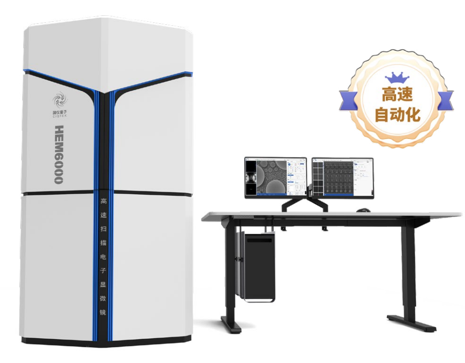
The HEM6000 High-Speed Scanning Electron Microscope (SEM) redefines industrial and scientific imaging by merging ultrafast acquisition speeds with nanometer-level resolution, enabling cross-scale large-area sample analysis for applications ranging from semiconductor manufacturing to materials science. Engineered for efficiency and precision, it outperforms conventional field-emission SEMs with a 5x faster imaging speed, making it the ultimate tool for high-throughput research and quality control.
Core Technological Advantages
The HEM6000 integrates six breakthrough technologies to deliver unmatched performance:
High-Speed Scanning Driver: Achieves 10 ns/pixel dwell time and 2×100M pixel/s acquisition speed, enabling millisecond-level imaging of dynamic samples.
Electron Filtering System: Freely switches between Secondary Electron (SE) and Backscattered Electron (BSE) signals, with adjustable mixing ratios for enhanced contrast in complex materials.
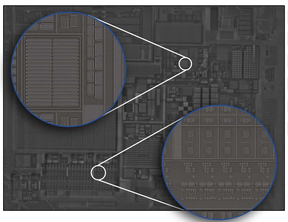
All-Electrostatic High-Speed Deflection System: Enables high-resolution large-field imaging (4 nm pixel size, 32 μm×32 μm max field of view) with minimal distortion.
Sample Stage Deceleration Technology: Reduces landing voltage of incident electrons while boosting recycled electron collection efficiency, critical for low-voltage high-resolution imaging.
Immersion Electromagnetic Compound Objective Lens: Uses magnetic field immersion to minimize aberrations, achieving 1.3 nm resolution @3 kV (SE) and 2.2 nm @1 kV (SE).
High-Brightness Large-Current Electron Gun: Ensures stable electron emission for consistent imaging across varying sample types.
Key Performance Specifications
Imaging Speed: 10 ns/pixel dwell time; 2×100M pixel/s maximum acquisition rate (5x faster than conventional SEMs).
Accelerating Voltage: 100V–6kV (deceleration mode) for low-voltage high-resolution; 6kV–30kV (non-deceleration mode) for deep penetration.
Resolution: 1.3 nm @3 kV (SE), 2.2 nm @1 kV (SE); 1.9 nm @3 kV (BSE), 3.3 nm @1 kV (BSE).
Field of View: Max 1×1 mm²; high-res micro-distortion field 32×32 μm².
Sample Stage: Motor-driven 3-axis stage (X/Y: 110mm travel, Z: 28mm); ±0.6 μm (X)/±0.3 μm (Y) repeatability.
Vacuum System: Fully automated oil-free vacuum for contamination-free operation.
Intelligent Automation & Applications
The HEM6000 features a high-speed automation workflow with full-auto sample loading/unloading (<15 min cycle time), auto-focus, auto-brightness/contrast, and auto-stitching. Its large-field low-distortion design follows dynamic scanning field axes to minimize edge blur, while low-voltage high-resolution capability (via sample stage deceleration) preserves delicate samples.
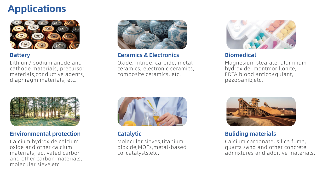
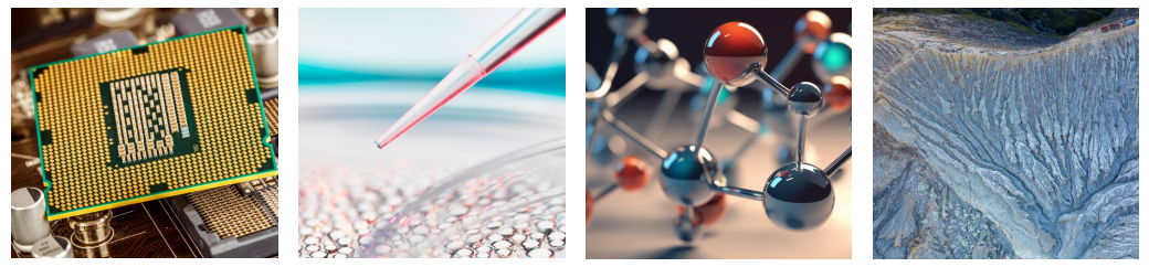
Applications span:
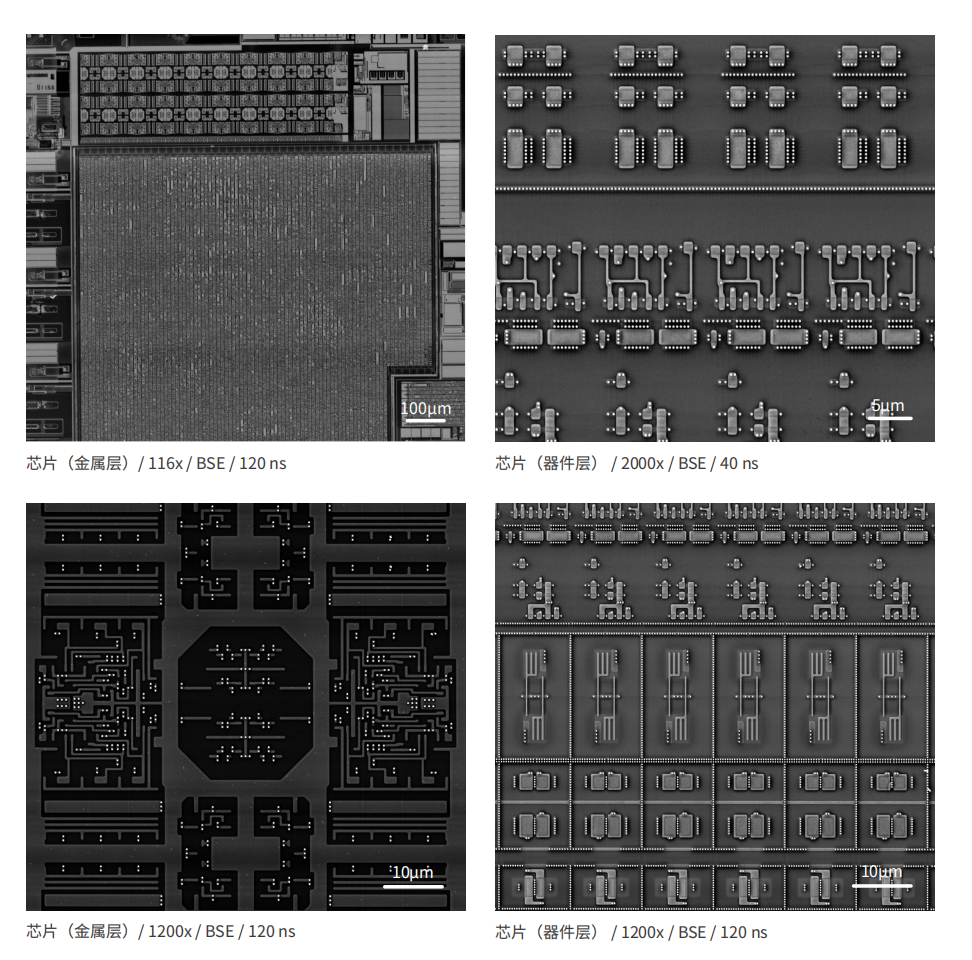
Semiconductor Industry: Wafer defect analysis, packaging inspection.
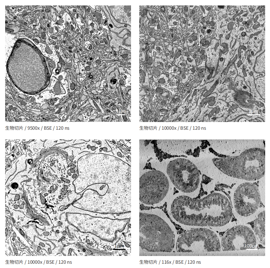
Life Sciences: Cell/tissue morphology studies.
Material Science: Nanostructure characterization, composite material analysis.
Geological Science: Mineral composition and fracture analysis.
Software & Expandability
The system runs on Windows OS with Chinese/English support, offering optical/gesture navigation, AI noise reduction (optional), 3D reconstruction, and big-data analysis. Standard detectors include in-lens SE/BSE detectors; optional upgrades feature plasma cleaning, 6-inch sample holders, and active vibration damping.
SEO Core Keywords
High-Speed Scanning Electron Microscope HEM6000
Nanometer Resolution SEM
Automated SEM Imaging System
Cross-Scale Large-Area SEM
Low-Voltage High-Resolution SEM
SEM with 5x Faster Imaging Speed
Industrial SEM for Semiconductor Inspection
Scientific SEM for Material Science
Automated Sample Loading SEM
High-Brightness Electron Gun SEM