

DB550 Ga+ Focused Ion Beam Field Emission Scanning Electron Microscope
The DB550 integrates a Ga+ Focused Ion Beam (FIB) column with a Field Emission SEM, featuring "Super Tunnel" electron optics (low aberration, magnetic-free lens), 3nm@30kV ion resolution, and 0.9nm@15kV SEM resolution. It includes a nanomanipulator (≤10nm precision), gas injection system (single GIS, ±0.1°C temp control), and 8-inch compatible loadlock. Ideal for nano-fabrication, semiconductor failure analysis, and materials characterization with automated workflows and expandable detectors (EDS/EBSD/STEM).
DB550 Ga+ Focused Ion Beam Field Emission Scanning Electron Microscope Applications and Related Testing Solutions
DB550 Ga+ Focused Ion Beam Field Emission Scanning Electron Microscope supports precision inspection and analysis tasks that require clear imaging, stable test conditions, and dependable laboratory or production quality control.
Related Products: Scanning NV Microscope | EASY-G 1310M Gas Pycnometer | Specific Surface & Porosimetry Analyzer EASY-V
Core Technological Advantages
The DB550’s superiority stems from five key innovations:
"Super Tunnel" Electron Optics: Features in-column beam deceleration to reduce spatial charge effects, enabling low-voltage (20V–30kV) high-resolution imaging with minimal aberrations.
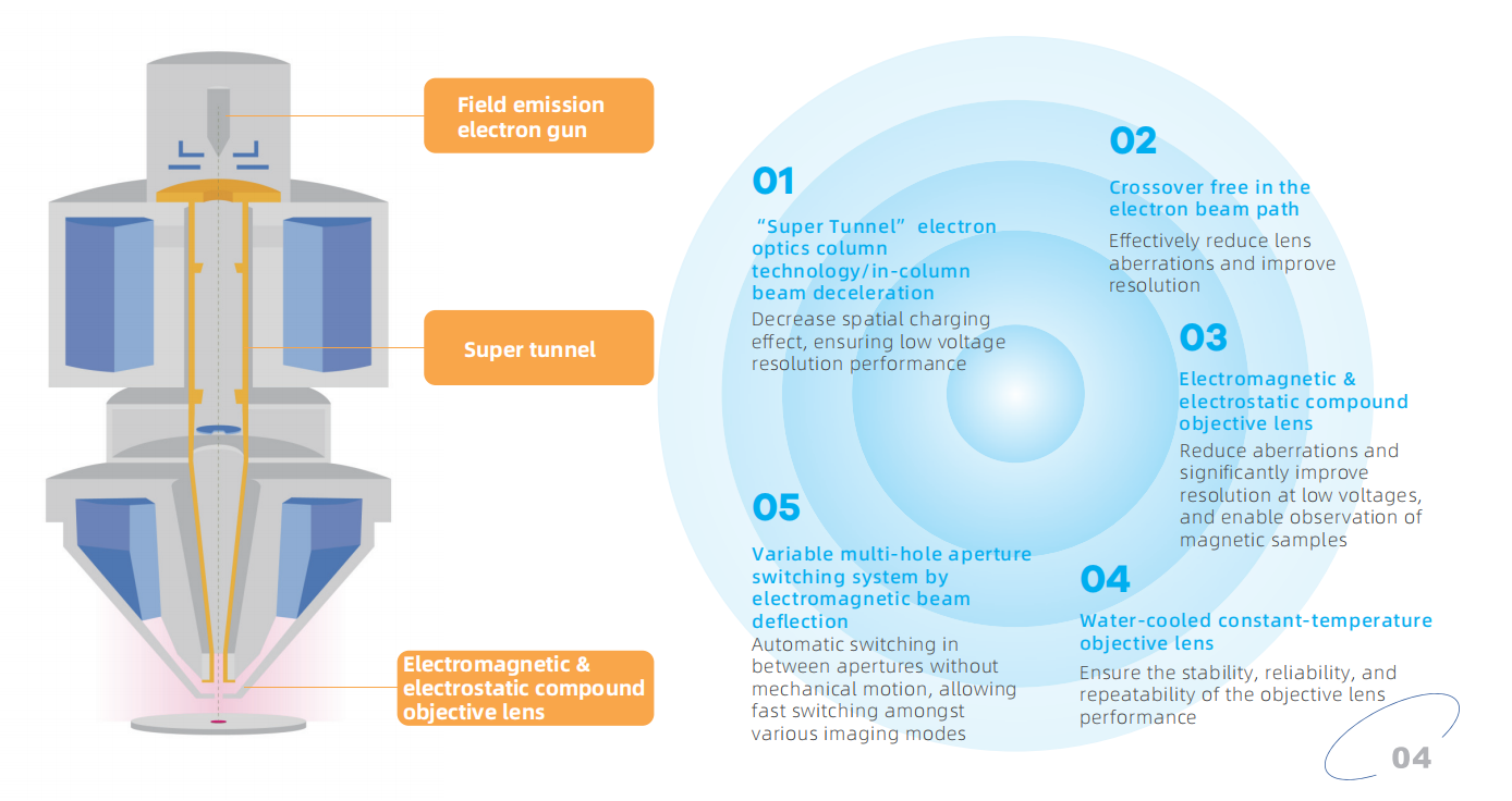
Crossover-Free Path: Eliminates beam crossovers to enhance resolution and reduce lens distortions, critical for sub-nanometer feature analysis.
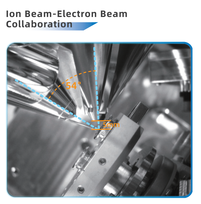
Electromagnetic & Electrostatic Compound Objective Lens: Supports low-voltage (1kV) imaging with 1.6nm resolution, while enabling observation of magnetic samples—unachievable with conventional SEMs.
Water-Cooled Constant-Temperature Lens: Ensures stability and repeatability during long-term experiments, with automatic aperture switching for rapid mode transitions.
Variable Multi-Hole Aperture System: Uses electromagnetic deflection for seamless switching between imaging modes (e.g., secondary electron, backscattered electron) without mechanical adjustments.
Key Components & Performance
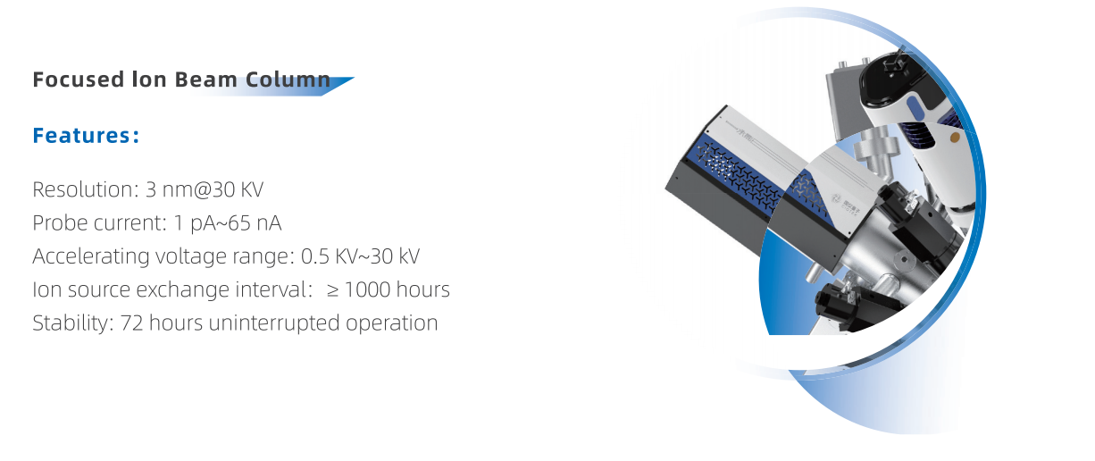
Focused Ion Beam (FIB) Column:- Resolution: 3nm@30kV (Ga+ ion beam), with probe currents from 1pA to 65nA for delicate milling or bulk material removal.
Stability: 72-hour uninterrupted operation, ion source exchange interval ≥1000 hours, and acceleration voltage range of 0.5kV–30kV.
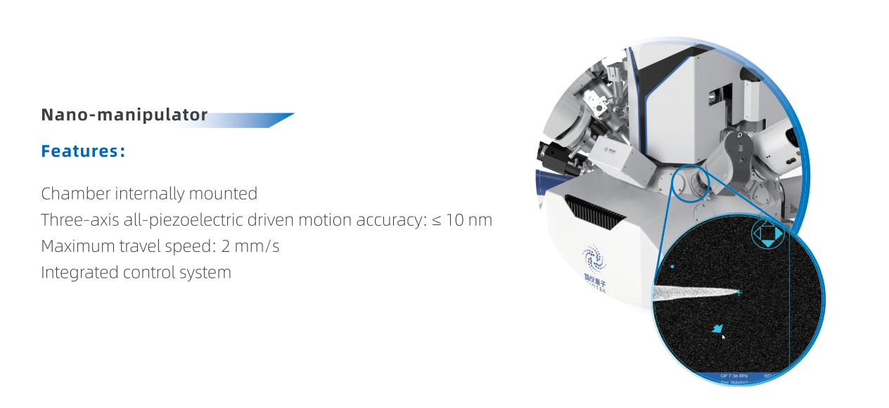
Nanomanipulator:
Chamber-mounted, three-axis all-piezoelectric driven system with ≤10nm motion accuracy and 2mm/s maximum speed. Ideal for precise sample positioning and in-situ manipulation.
Gas Injection System (GIS):
Single GIS design with multiple precursor gases (e.g., platinum, tungsten for deposition), distance ≥35mm, and motion repeatability ≤10μm. Heating control (room temp–90°C) with ±0.1°C precision ensures consistent chemical reactions.
Applications Across Industries
Semiconductor:
IC chip failure analysis via cross-sectional milling, TEM specimen preparation (lamella thinning), and circuit editing. Critical for debugging advanced nodes (e.g., 7nm/5nm).
New Energy:
Lithium-ion battery material characterization: Morphology observation, particle size analysis, and failure diagnostics (e.g., dendrite growth) using BSE/EDX/SIMS.
Ceramic Materials:
High-precision micro-nano machining (e.g., trench etching) paired with 3D imaging via BSE/EDX/EBSD/SIMSables study of grain boundaries and phase distributions (scale: 2–5μm).
Alloy Materials:
Reinforced phase analysis (e.g., metal-matrix composites) using FIB-prepared TEM specimens for transmission Kikuchi diffraction (TKD) and in-situ mechanical testing.
Technical Specifications
Electron Optics:
Gun: High-brightness Schottky field emission electron gun.
Resolution: 0.9nm@15kV (high contrast), 1.6nm@1.0kV (high resolution).
Acceleration Voltage: 20V–30kV (variable).
Ion Beam System:
Source: Ga+ liquid metal ion source.
Resolution:nm@30kV; acceleration voltage 500V–30kV.
Specimen Chamber:
Vacuum: Fully automated oil-free system.
Stage: Motorized 5-axis eucentric stage (X/Y=110mm, Z=65mm; tilt -10°–+70°, rotation 360°).
Cameras: 3x (1x optical navigation + 2x monitoring).
Detectors & Options:
Standard: In-lens electron detector, Everhart-Thornley Detector (ETD).
Optional: BSD, STEM, EDS, EBSD, nanomanipulator, plasma cleaner, 8-inch loadlock.
User Interface:
Windows OS with optical/gesture navigation; autoocus/stigmator functions.
Competitive Edge
Compared to conventional FIB-SEMs, the DB550 offers:
Higher Throughput: Automated workflows (sample loading, alignment) reduce setup time by 40%.
Enhanced Flexibility: Expandable detector suite supports multi-modal analysis (e.g., EDS for elemental mapping + EBSD for crystallography).
Industrial-Grade Reliability: Water-cooled lens and oil-free vacuum ensure 24/7 operation in cleanrooms.
SEO Keywords
DB550 Ga+ Focused Ion Beam SEM
Integrated FIB-SEM workstation
Super Tunnel electron optics
Nano-fabrication SEM
Semiconductor failure analysis tool
Low-voltage high-resolution SEM
Gas injection system GIS
Nanomanipulator precision tool
Materials characterization FIB-SEM
8-inch compatible specimen loadlock