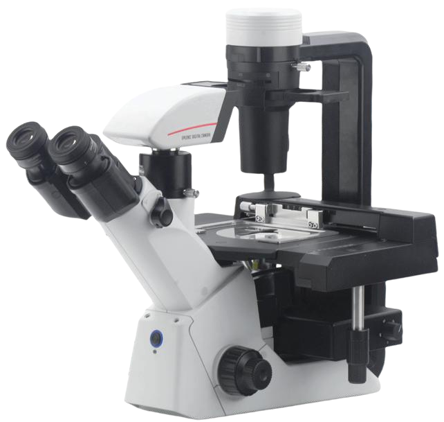


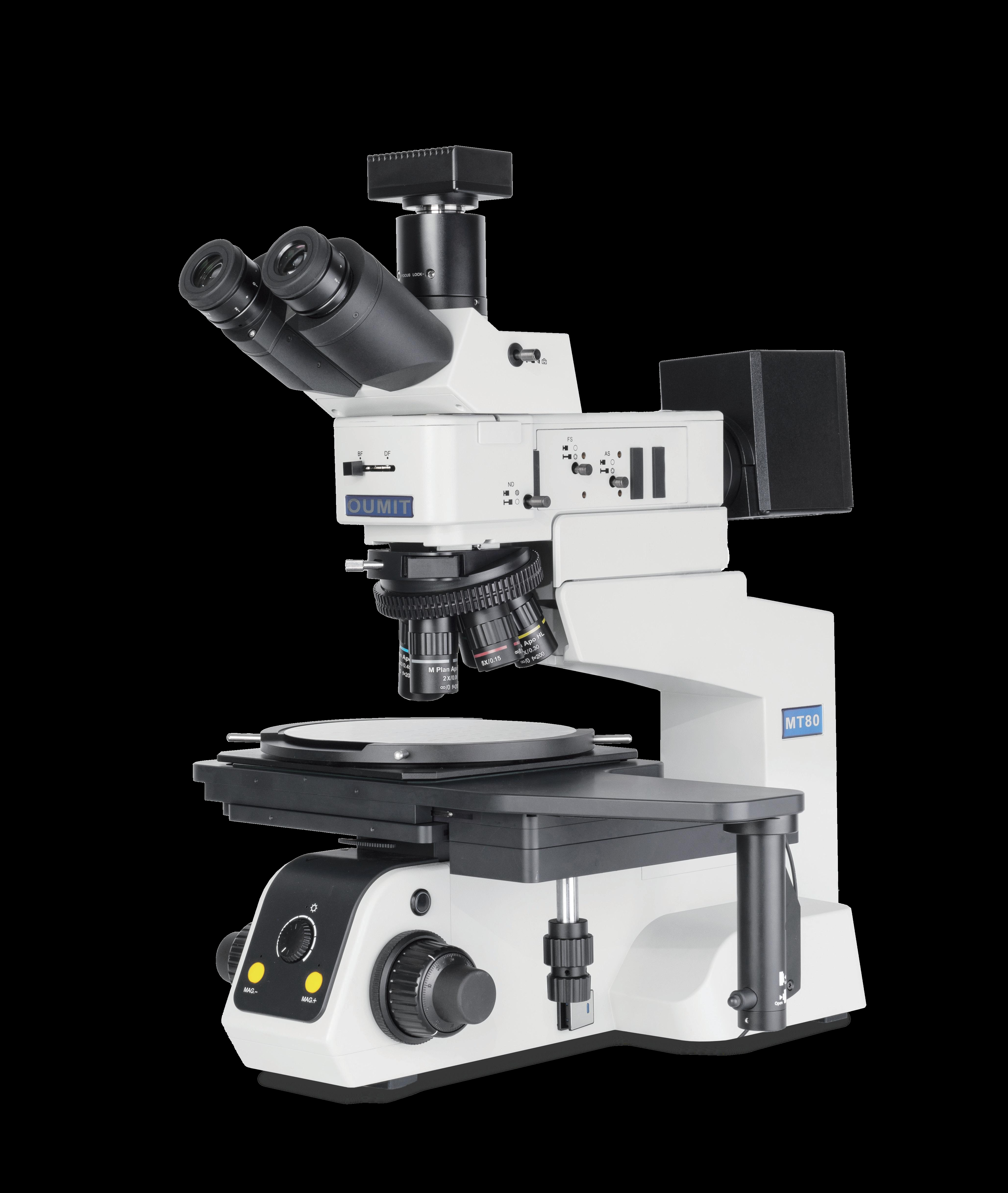
Omitek APO Long Working Distance Metallurgical Microscope MT12/80/60/40L
Omitek’s APO Long Working Distance Metallurgical Microscope MT12/80/60/40L bridges the market gap with high magnification and ultra - long working distance. It excels in high - cavity component inspection (microwave devices, semiconductors,
Omitek APO Long Working Distance Metallurgical Microscope MT12/80/60/40L Applications and Related Testing Solutions
Omitek APO Long Working Distance Metallurgical Microscope MT12/80/60/40L supports precision inspection and analysis tasks that require clear imaging, stable test conditions, and dependable laboratory or production quality control.
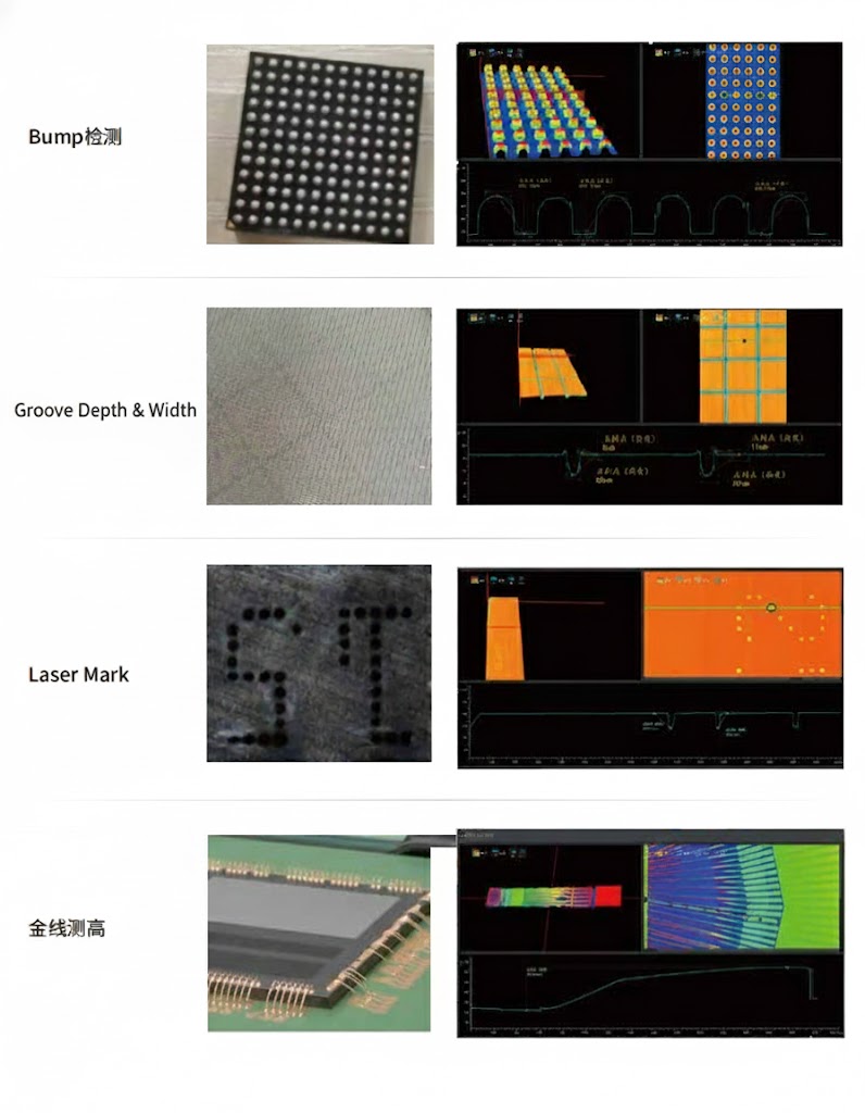
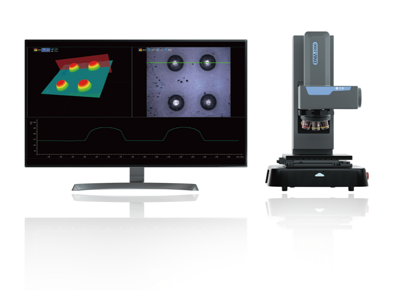
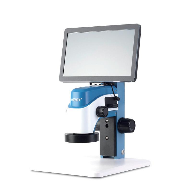
Related Products: MTS Series Spectral Confocal 3D Topography Measurement System | DMZ1000 Series Microscopic Automation System | Video Integrated Machines TV - 03 & TV - 04
Key Technical Advantages
Advanced Optical System
It is equipped with APO (Apochromatic) long - working - distance objective lenses. For example, there are 2X/NA0.06/WD34, 5X/NA0.15/WD45, 10X/NA0.3/WD34, 20X/NA0.3/WD31, and optional 50X NA0.45/WD21, 100X NA0.80/WD6 lenses. These lenses can provide sharp images without chromatic aberration even at high magnification, while still maintaining a large working distance for flexible operation.
An infinite tube length and infinity - corrected optical system are adopted, which ensures bright and clear imaging across the entire field of view. There is no need for frequent optical correction during use.
Versatile Observation Modes
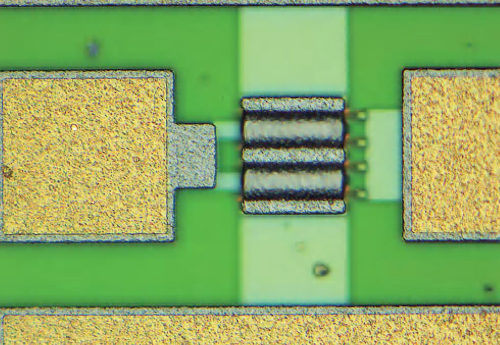
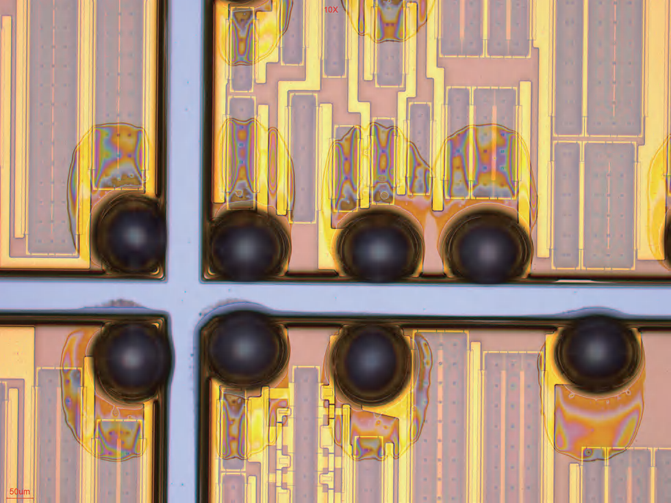
It supports brightfield, darkfield, polarized light (P), and Differential Interference Contrast (DIC) imaging. This wide range of imaging modes enables precise inspection of surface topography, defects, and material heterogeneity in semiconductor chips, FPDs, circuit boards, and precision molds. For instance, the DIC mode can enhance the detection of micro - cracks or layer delamination by improving edge detection.
Large - Scale Sample Platforms
There are 4”, 6”, 8”, 10”, and 12” platform sizes available to accommodate various wafer dimensions, from small semiconductor dies to large FPD substrates. The stage supports manual/X/Y/Z - axis movement. The travel range for focus adjustment is 50mm–76mm, and for XY positioning is 210mm×210mm. Fine - tuning knobs ensure micrometer - level accuracy, which is essential for stable sample placement during critical inspections like probe station alignment.
Intelligent & Efficient Workflow
AI image recognition is integrated into the microscope to automate defect detection, measurement, and data logging. When used with Omitek’s software suite, it simplifies quality control. It can instantly identify anomalies in solder joints, coating uniformity, or die bonding, reducing human error and speeding up inspection cycles.
Industrial - Grade Design
Illumination: It uses Köhler illumination with a 10W LED light source (brightness adjustable), providing uniform and flicker - free lighting for consistent imaging. Optional darkfield/DIC modules can further enhance contrast.
Focus System: Coarse/fine focus knobs with click - stop adjustment allow for precise Z - axis control (resolution: 0.001mm), which is crucial for resolving nanoscale features in advanced semiconductors.
Durability: Designed for 24/7 industrial use, it has robust mechanics such as anti - vibration stage mounts and sealed optical pathways to withstand harsh manufacturing environments.
Industry Applications
Semiconductor Sector: Used in probe station operations (die bonding inspection, solder paste volume measurement), wafer - level packaging (WLP) defect analysis, and MEMS device characterization.
Optoelectronics: Inspects TO - can lasers, butterfly package components, and optical fiber connectors.
Consumer Electronics: Detects defects in FPD (LCD/OLED) panels, controls the quality of touch sensors, and inspects PCB substrate lamination.
Precision Manufacturing: Verifies the hermetic seal of ceramic capacitors, the assembly of filter modules, and the texturing of high - end molds.
Why Choose This Model?
Unlike traditional metallographic microscopes, the MT12/80/60/40L balances high magnification (up to 100X) with unrestricted working space due to its ultra - long WD. This makes it indispensable for tasks that require both detail and maneuverability, such as semiconductor probing, manual marking, or cleanroom operations where sample repositioning must be error - free. Its modular design also allows for customization with accessories like motorized stages, high - resolution cameras, and data analysis software, preparing for automated inspection lines in the future.
Maintenance & Support
Omitek offers comprehensive after - sales service:
Calibration certification for optical components to ensure metrological accuracy.
Training programs on software operation, including image analysis and AI algorithm configuration.
Fast availability of spare parts for critical components (objective lenses, illumination modules).
Conclusion
The APO Long Working Distance Metallurgical Microscope MT12/80/60/40L redefines precision inspection for high - value, high - cavity components. By combining cutting - edge optics, intelligent automation, and industrial durability, it helps manufacturers achieve zero - defect quality control in semiconductor, optoelectronics, and advanced manufacturing processes.
SEO Hot Keywords
apo metallurgical microscope, long working distance microscope, semiconductor inspection microscope, high magnification microscope, DIC microscopy, brightfield darkfield microscope, wafer inspection tool, microchip testing equipment, omitek microscopy, industrial metallographic microscope, AI microscopy, probe station microscope, optical inspection machine, microelectronics testing equipment