


What is a Scanning Electron Microscope?
What is a Scanning Electron Microscope?
A Scanning Electron Microscope (SEM) is a powerful analytical instrument that produces highly detailed, high-magnification images of a sample's surface by scanning it with a focused beam of electrons, rather than light. It overcomes the fundamental resolution limit of optical microscopes, allowing scientists and engineers to visualize and analyze structures at the nanometer scale—far smaller than what is visible to the naked eye or with standard microscopes. The core principle of an SEM involves generating a beam of primary electrons in a high vacuum, focusing it into a fine probe using electromagnetic lenses, and raster-scanning this probe across the sample surface. The interaction between the energetic electron beam and the sample generates a variety of signals, including secondary electrons (SE) for topographical contrast and backscattered electrons (BSE) for compositional (atomic weight) contrast. By detecting and mapping these signals, an SEM constructs a detailed, pseudo-3D image of the surface morphology. This capability makes it an indispensable tool for materials science, failure analysis, nanotechnology, and biological research, providing insights that are critical for product development, quality control, and scientific discovery. For research and industrial labs, accessing advanced imaging technology through reliable suppliers is key to maintaining a competitive edge in analysis.
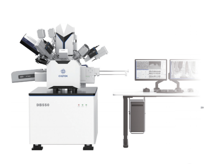
How Does an SEM Work: The System and Signal Generation
The operation of an SEM relies on a sophisticated, integrated system. It begins with the electron gun (thermionic or field emission), which emits a stream of primary electrons. These electrons are accelerated by a high voltage (typically 0.1 kV to 30 kV) and focused by a series of electromagnetic condenser and objective lenses into an extremely fine probe, sometimes just a few nanometers in diameter. A critical requirement is a high vacuum system within the column and sample chamber to prevent electron scattering by air molecules and to protect the filament. The focused probe is then scanned across the sample surface in a precise raster pattern by scanning coils. When the high-energy electrons strike the sample, they interact with its atoms, generating the key signals. Secondary electrons (SE), which are low-energy electrons ejected from the sample's surface atoms, are highly sensitive to surface topography and provide the familiar, depth-rich 3D-like images. Backscattered electrons (BSE) are primary electrons that are elastically scattered back after interacting with atomic nuclei; their yield increases with the atomic number of the sample, providing contrast between areas of different chemical composition. Specialized detectors (e.g., Everhart-Thornley for SE, solid-state for BSE) capture these signals, which are then amplified and synchronized with the scan to build a pixel-by-pixel image on a display monitor. Modern digital SEMs, like those from advanced technology providers, offer precise control over all these parameters for optimal imaging.
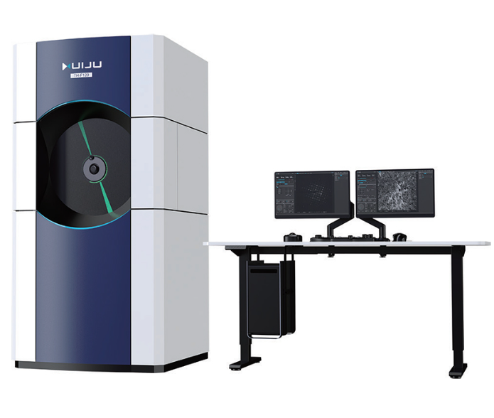
Key Applications and the Power of Integrated Analysis
The true power of an SEM extends far beyond capturing stunning high-resolution images. Its primary application is in materials characterization, where it is used to examine the microstructure of metals, ceramics, polymers, and composites, revealing grain boundaries, phases, porosity, and cracks. In failure analysis, an SEM can pinpoint the origin of a fracture, identify contamination, or analyze wear mechanisms in faulty components. A transformative capability comes from integrating an Energy Dispersive X-ray Spectroscopy (EDS or EDX) detector. When the electron beam excites a sample's atoms, they emit characteristic X-rays. The EDS system collects and analyzes these X-rays to determine the elemental composition of the sample, down to trace levels, and can create element distribution maps. This combination of high-resolution imaging and chemical microanalysis is revolutionary. It allows researchers to not only see a tiny particle or inclusion but also instantly know what elements it contains. This is critical in fields like geology (mineral identification), forensics (evidence analysis), semiconductor manufacturing (defect review), and pharmaceuticals (contaminant identification). The ability to perform such comprehensive analysis in a single instrument makes the SEM-EDS system a cornerstone of modern analytical laboratories, driving innovation and ensuring quality across countless industries.
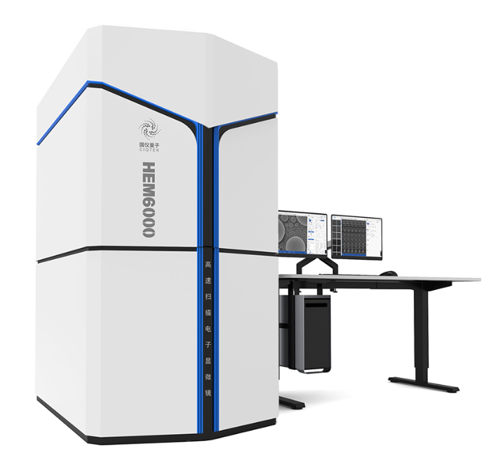
A Scanning Electron Microscope is a window into the micro- and nanoworld, using a focused beam of electrons to reveal intricate surface details and compositional information invisible to light. By translating electron-sample interactions into detailed images and elemental data, the SEM, especially when coupled with EDS, provides an unparalleled analytical capability. It is an essential instrument for advancing research, solving complex engineering problems, and ensuring the integrity of materials and products in today's technology-driven world.