


The Role of Scanning Electron Microscopes in Material Science and Nanotechnology
The Role of Scanning Electron Microscopes in Material Science and Nanotechnology
Unmatched Imaging Capabilities: Revealing the Micro and Nano World
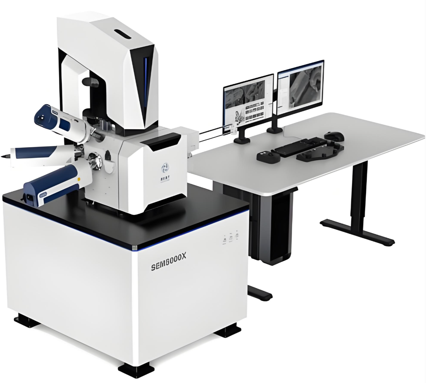
The Scanning Electron Microscope (SEM) stands as a cornerstone instrument in material science and nanotechnology, primarily due to its unparalleled imaging capabilities. Unlike optical microscopes limited by light diffraction, SEM utilizes a focused beam of high-energy electrons scanned across a specimen's surface. The interaction between these electrons and the sample generates various signals, including Secondary Electrons (SE), which are most commonly used for imaging. SE imaging provides exceptional topographical contrast and spatial resolution down to the nanometer scale (typically 1-20 nm), allowing researchers to visualize surface textures, grain boundaries, particle morphology, and microstructural features with breathtaking clarity. This deep, three-dimensional-like view of surfaces is indispensable for characterizing everything from fracture surfaces in metallurgy and the layered structure of composite materials to the intricate architecture of nanoparticles and the precise patterning of semiconductor circuits. The ability to image at these magnifications (from 10x up to 1,000,000x) makes the SEM an essential tool for visualizing the very building blocks and defects that dictate material properties and device performance.
Beyond Imaging: Elemental Analysis and Advanced Characterization
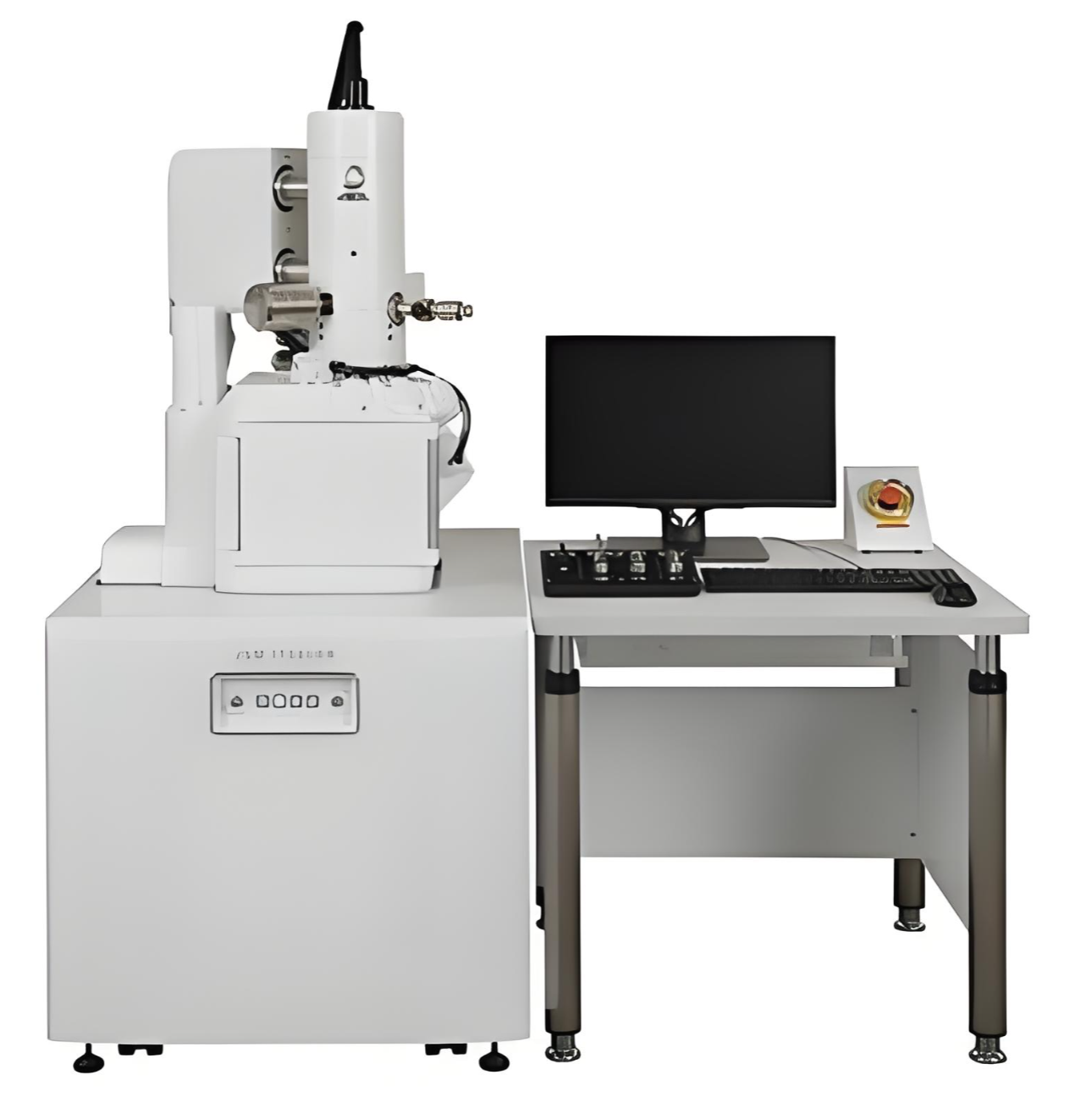
The power of the SEM extends far beyond mere high-resolution imaging. By detecting the Backscattered Electrons (BSE) and characteristic X-rays emitted during electron-sample interactions, the SEM transforms into a powerful analytical tool. Backscattered Electron Imaging provides atomic number contrast (Z-contrast), where brighter areas correspond to elements with higher atomic numbers. This allows for the easy distinction between different phases in a material, such as identifying inclusions in a metal matrix. The most significant analytical leap comes with the integration of Energy Dispersive X-ray Spectroscopy (EDS or EDX). An EDS detector captures the characteristic X-rays, enabling qualitative and quantitative elemental analysis of microscopic features. Researchers can pinpoint the elemental composition of a specific grain, a contamination spot, or a thin coating, mapping the distribution of elements across a sample surface. This combination of high-resolution imaging with in-situ chemical analysis is critical for solving complex materials problems, such as identifying the cause of corrosion, verifying the purity of synthesized nanomaterials, or analyzing the composition of failure sites in electronic components.
Driving Innovation in Nanotechnology and Advanced Materials Development
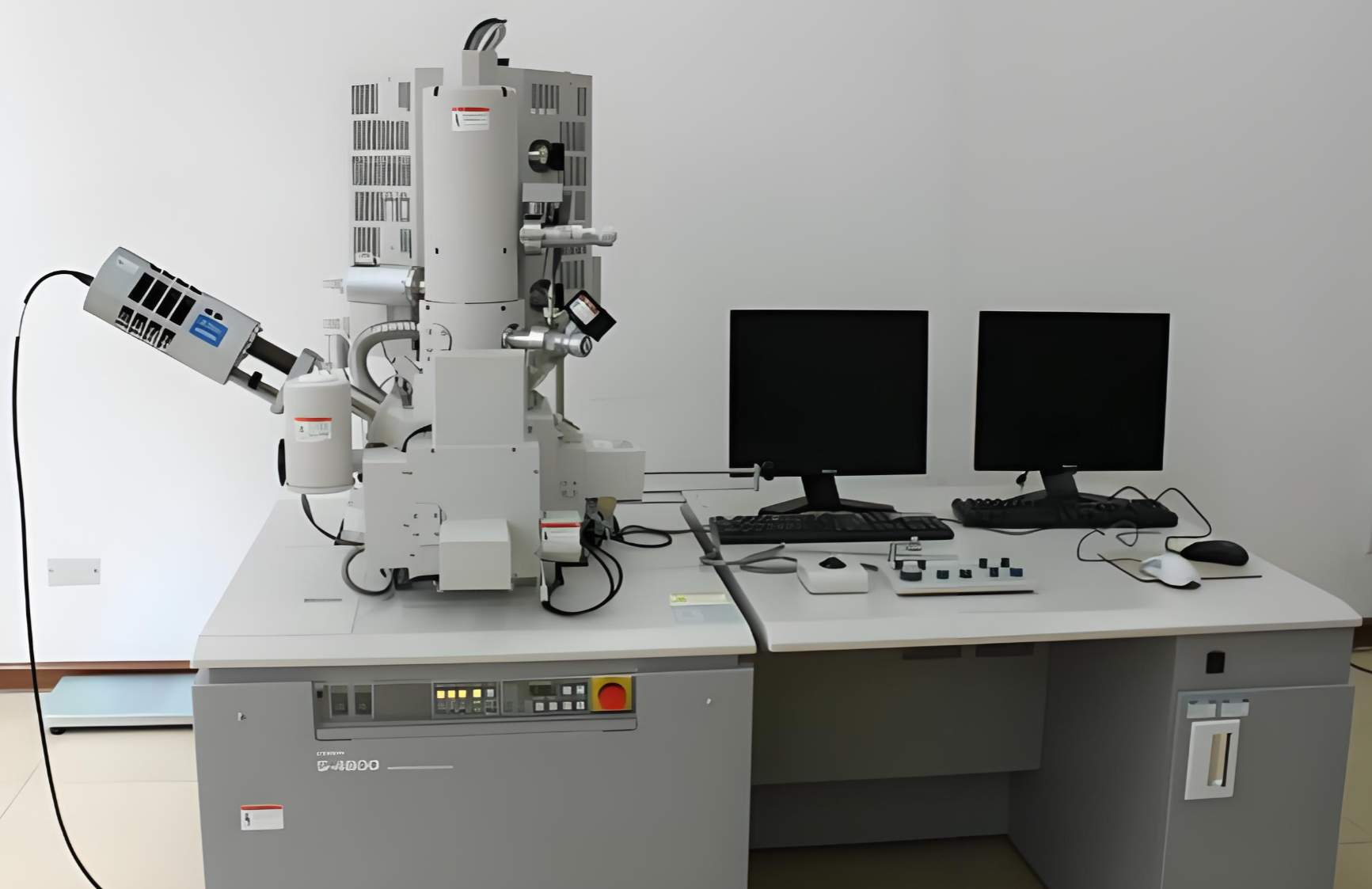
In the realms of nanotechnology and advanced materials engineering, the SEM is not just an observational tool but an active driver of research, development, and quality control. It enables the precise characterization of nanomaterials—measuring nanoparticle size distribution, assessing the aspect ratio of nanotubes or nanowires, and examining the porosity of nanostructured scaffolds for medical or energy applications. For thin-film technologies and semiconductor fabrication, SEM is vital for process control and defect review, inspecting lithographic patterns, layer thicknesses, and identifying sub-micron defects that could cripple device yield. Furthermore, advanced SEM techniques like Electron Backscatter Diffraction (EBSD) provide crystallographic information, mapping grain orientation and phase distribution, which is essential for understanding and optimizing material properties like strength, conductivity, and magnetic behavior. Access to reliable SEM technology and expertise, facilitated by suppliers like Skyline International, empowers R&D teams and quality labs to innovate with confidence, validate new material designs, troubleshoot production issues, and push the boundaries of what is possible at the micro and nanoscale.
The Scanning Electron Microscope is an indispensable pillar in modern material science and nanotechnology. By providing unprecedented visualization of micro and nanoscale structures and coupling it with powerful chemical and crystallographic analysis, the SEM delivers the comprehensive insights needed to understand material behavior, innovate new products, and ensure manufacturing quality. From fundamental research exploring novel nanomaterials to industrial quality control on high-tech production lines, the SEM's role in illuminating the hidden details that govern material performance is irreplaceable, making it a critical investment for any organization operating at the forefront of technology and materials development.