


How C-SAM Scanning Acoustic Microscopy Detects Hidden Defects in Semiconductor Packages
How C-SAM Scanning Acoustic Microscopy Detects Hidden Defects in Semiconductor Packages
The Principle of Acoustic Imaging: Seeing Through Opaque Materials
Scanning Acoustic Microscopy (C-SAM) operates on a fundamentally different principle than optical microscopy. Instead of light, it utilizes high-frequency ultrasonic waves (typically 5 MHz to 300 MHz) as its probing medium. A transducer generates these sound waves, which are coupled into the semiconductor package via a water immersion medium. As the ultrasonic pulse travels through the different materials within the package—such as the silicon die, adhesive layers, lead frame, and molding compound—it encounters interfaces and internal features. At each material boundary, a portion of the sound wave is reflected back to the transducer due to changes in acoustic impedance (a property dependent on material density and stiffness). By precisely scanning the transducer across the sample and analyzing the time-of-flight and amplitude of these returning echoes, C-SAM constructs a detailed, layer-by-layer internal image. This allows it to "see through" optically opaque materials like epoxy molding compounds, metals, and ceramics, revealing subsurface and internal structures without any destructive disassembly, making it an indispensable non-destructive inspection (NDI) tool.
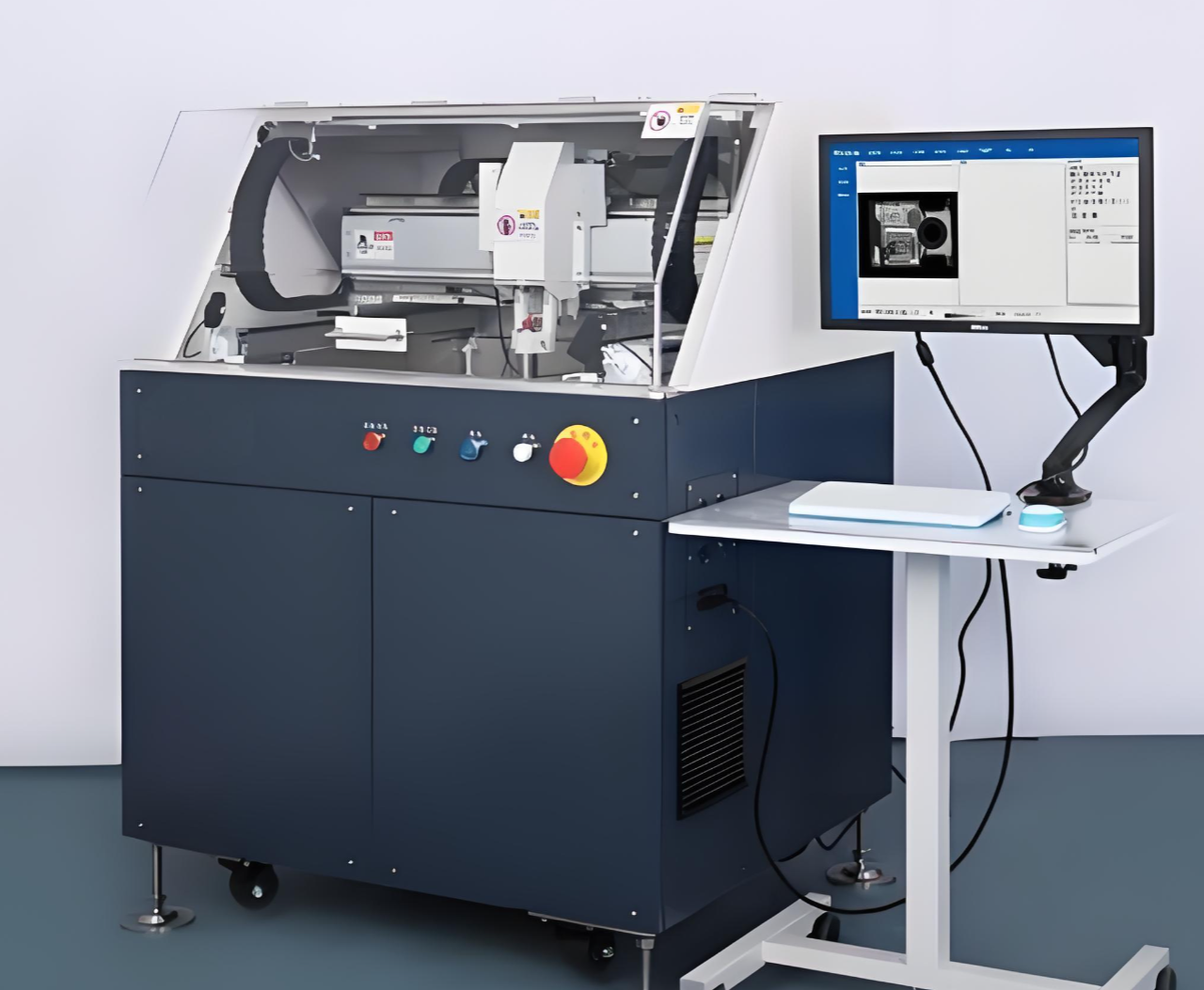
Identifying Critical Failure Modes: Voids, Delamination, and Cracks
The true power of C-SAM lies in its exceptional sensitivity to specific types of defects that are catastrophic for semiconductor reliability but invisible to X-ray or optical inspection. Its primary applications target key failure modes. Delamination is a major concern; it refers to the separation at the interfaces between different materials, such as between the die and the die attach material, or between the molding compound and the lead frame. C-SAM clearly reveals these gaps as bright white (high reflection) or dark (signal loss) areas, depending on the imaging mode. Voids or porosity within the die attach adhesive or underfill material are also readily detected. These air bubbles can lead to thermal hotspots and mechanical stress, impairing performance and longevity. Furthermore, C-SAM can detect cracks within the silicon die or the molding compound itself. By using different analysis modes like Through-Scan or non-destructive cross-sectioning, analysts can pinpoint the exact depth and location of these hidden flaws, providing critical data for root cause analysis in packaging processes such as wire bonding, molding, and reflow soldering.
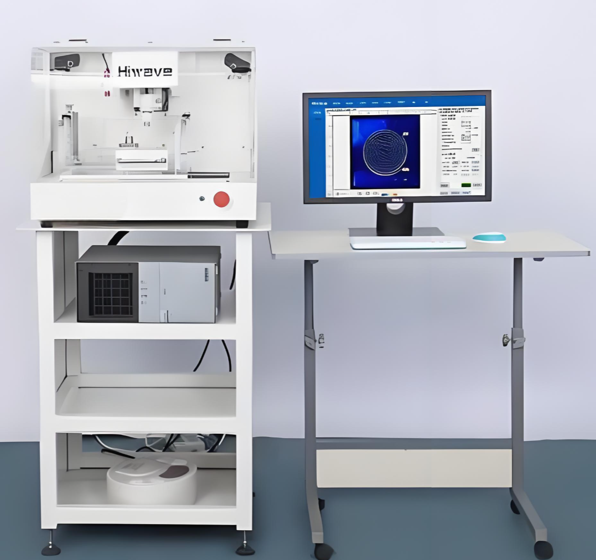
Application in Quality Assurance and Failure Analysis
C-SAM is integrated at multiple stages of the semiconductor product lifecycle, serving as a cornerstone for quality assurance and advanced failure analysis. In incoming quality control (IQC), it screens raw materials like substrates and laminated packages for pre-existing flaws. During process qualification and monitoring, it is used to optimize and validate critical packaging processes (e.g., molding parameters, die attach epoxy dispensing) by checking for defect formation. For reliability testing, samples subjected to environmental stresses—such as Temperature Cycling, Highly Accelerated Stress Test (HAST), or Pressure Cooker Test (PCT)—are inspected with C-SAM before and after to assess whether delamination or cracking has been induced. Finally, in failure analysis (FA) of returned or field-failed units, C-SAM provides the first non-destructive look inside the package, guiding subsequent destructive physical analysis (DPA) to the exact area of interest. This capability prevents good units from being destroyed and dramatically accelerates the FA process. Suppliers like Skyline International facilitate this critical work by providing access to advanced C-SAM equipment and the technical support needed to interpret complex acoustic images accurately.
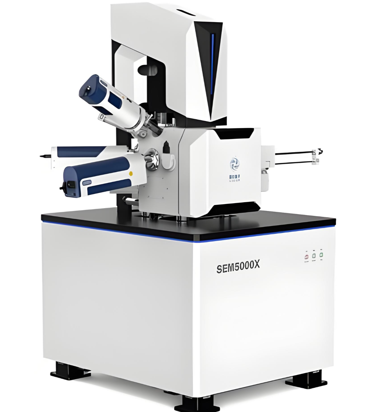
In the era of advanced, miniaturized, and high-reliability semiconductor packages, C-SAM is not merely an inspection tool but a vital insurance policy. It provides the unique ability to detect hidden, latent defects that threaten device integrity long before electrical failure occurs. By enabling non-destructive visualization of internal interfaces, C-SAM empowers manufacturers to improve process yields, validate package designs, ensure long-term reliability, and conduct precise failure analysis. For any company committed to delivering robust semiconductor solutions, integrating C-SAM into their quality and analysis workflow is an essential strategy for mitigating risk and building market trust.