


Applications of Scanning Electron Microscopes (SEM) in Advanced Material Research
Applications of Scanning Electron Microscopes (SEM) in Advanced Material Research
Unveiling Microstructural Secrets: From Nanostructures to Failure Analysis
At the heart of advanced material research lies the need to visualize and understand structure-property relationships at the micro and nanoscale. The Scanning Electron Microscope (SEM) is an indispensable tool for this, offering unparalleled depth of field and resolution far exceeding that of optical microscopes. Researchers utilize SEM to reveal critical microstructural features such as grain size and distribution in metals, phase boundaries in alloys, porosity in ceramics, and fiber orientation in composites. In the critical field of failure analysis, SEM is deployed to examine fracture surfaces, identifying tell-tale signs of the failure mode—whether it be brittle cleavage, ductile dimpling, fatigue striations, or stress corrosion cracking. This direct visualization provides irrefutable evidence that guides the improvement of material composition and processing techniques. For developers of new alloys, high-strength polymers, or advanced ceramics, SEM analysis is the first and most crucial step in diagnosing performance and directing iterative design, enabling targeted enhancements in mechanical properties like strength, toughness, and fatigue resistance.
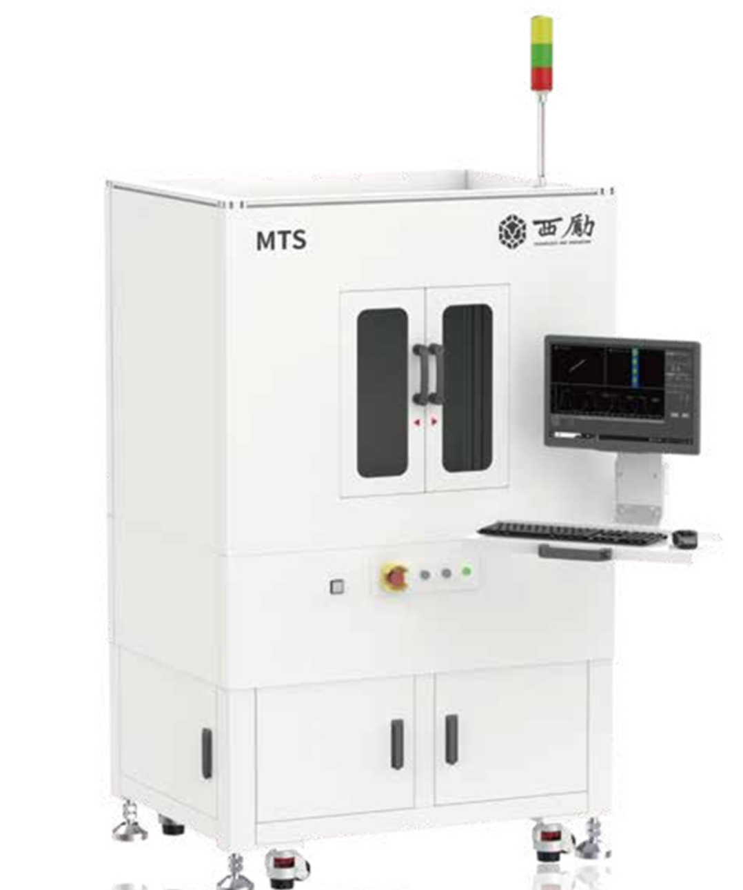
Elemental and Chemical Fingerprinting with Energy Dispersive X-ray Spectroscopy (EDS)
The true power of a modern SEM is magnified when coupled with Energy Dispersive X-ray Spectroscopy (EDS). While the SEM image reveals morphology, EDS detects the X-rays emitted from the sample when bombarded by the electron beam, providing qualitative and quantitative elemental analysis. This integrated capability is transformative for advanced material research. It allows scientists to map the distribution of elements across a surface, identifying segregations, inclusions, or contaminations that could compromise performance. For instance, in developing protective coatings or thin films, EDS can verify chemical composition and thickness uniformity. In studying corrosion or oxidation, it can identify the compounds formed on the surface. When analyzing composite materials or multi-phase systems, EDS precisely determines the chemical makeup of different phases. This synergy of high-resolution imaging and elemental analysis is critical for developing next-generation materials like high-entropy alloys, battery electrode materials, and semiconductor heterostructures, where precise chemical control at micro- and nano-domains dictates ultimate functionality.
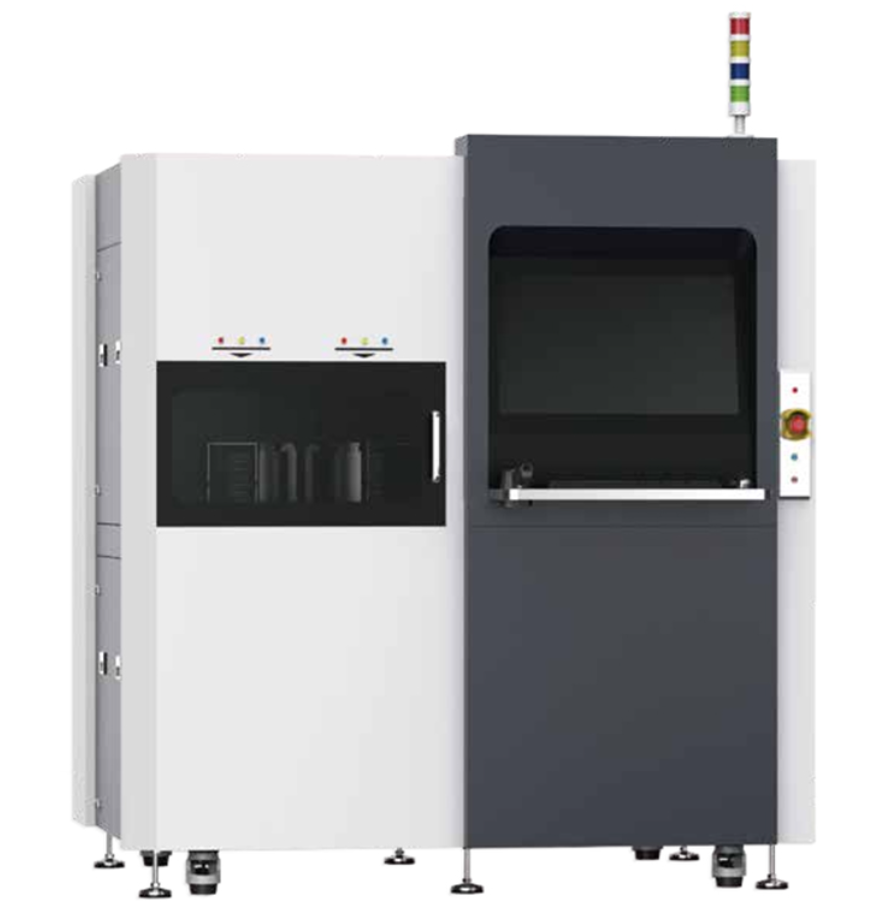
High-Resolution Imaging and In-Situ Experimentation
The frontier of SEM application in advanced research involves pushing the limits of resolution and integrating in-situ capabilities. High-resolution SEM (HR-SEM) and Field Emission SEM (FE-SEM) can resolve features down to the nanometer scale, making it possible to image nanoparticles, quantum dots, and the intricate pore structures of catalysts and filtration materials. Beyond static observation, advanced SEM stages enable in-situ experimentation, where the sample is subjected to controlled stimuli inside the microscope chamber. Researchers can perform in-situ tensile or heating stages, observing in real-time how a material's microstructure deforms, cracks propagate, or phases transform under stress or temperature change. This dynamic observation provides unprecedented insight into deformation mechanisms, thermal stability, and phase transition kinetics. For researchers designing materials for extreme environments or dynamic applications, such as aerospace components or energy storage devices, this in-situ SEM capability is invaluable for validating theoretical models and accelerating the development cycle from lab discovery to practical application.
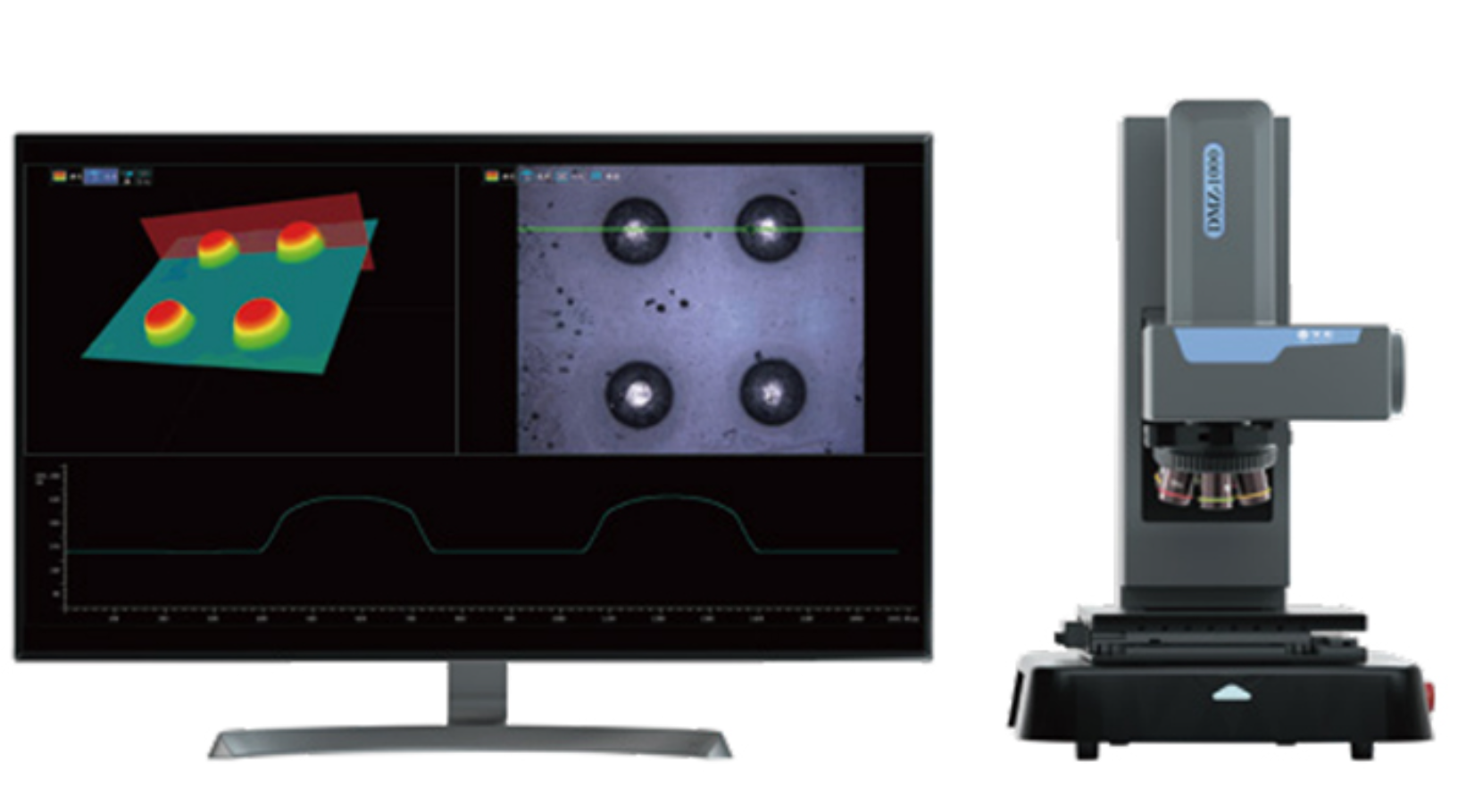
In summary, the Scanning Electron Microscope is a cornerstone of modern advanced material research. It transcends simple imaging to provide a comprehensive analytical platform for microstructural revelation, elemental mapping, and dynamic in-situ characterization. By offering deep insights into the intimate connections between a material's form, composition, and behavior under various conditions, SEM empowers researchers to design, diagnose, and optimize the high-performance materials that will define the future of technology and industry.