


The Role of Microhardness Testers in Semiconductor and Electronics Quality Control
The Role of Microhardness Testers in Semiconductor and Electronics Quality Control
Ensuring Material Integrity at the Microscale for Miniaturized Components
The relentless drive towards miniaturization in the semiconductor and electronics industries demands precision engineering at an almost atomic level. Components like wire bonding capillaries, micro-electro-mechanical systems (MEMS), and delicate connector pins have microscopic features where traditional hardness testing methods are impractical and destructive. This is where microhardness testers, specifically Vickers (HV) and Knoop (HK) scales, become indispensable. These instruments apply very low loads, ranging from 10gf to 1000gf, to create tiny, precisely measured indentations that are invisible to the naked eye. By analyzing these indentations under a high-powered optical microscope, engineers can obtain a quantitative measure of a material's hardness without compromising the component's structural integrity or functionality. This capability is critical for verifying the quality of raw materials, thin coatings, and heat-treated surfaces that are fundamental to the performance, reliability, and longevity of electronic devices.
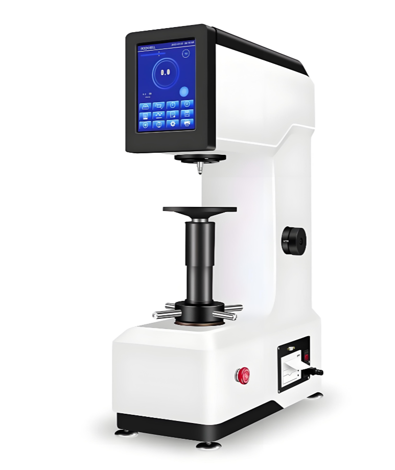
Validating Coating and Surface Treatment Efficacy for Enhanced Performance and Reliability
Many advanced electronics rely on specialized coatings and surface treatments to function correctly. Examples include gold plating on connectors for optimal conductivity, wear-resistant coatings on semiconductor tooling, and protective layers on substrates. Microhardness testing is the primary method for evaluating the effectiveness of these processes. It can measure the hardness of the coating itself to ensure it provides the necessary resistance to wear and corrosion. Crucially, through a technique known as cross-sectional microhardness testing, technicians can mount and polish a sample to reveal a cross-section, then perform a series of indentations from the coating surface down into the substrate. This creates a hardness profile, revealing the interdiffusion zone and verifying that the heat-affected zone (HAZ) possesses the required mechanical properties for robust adhesion and performance under thermal and mechanical stress, which is vital for preventing delamination and failure.
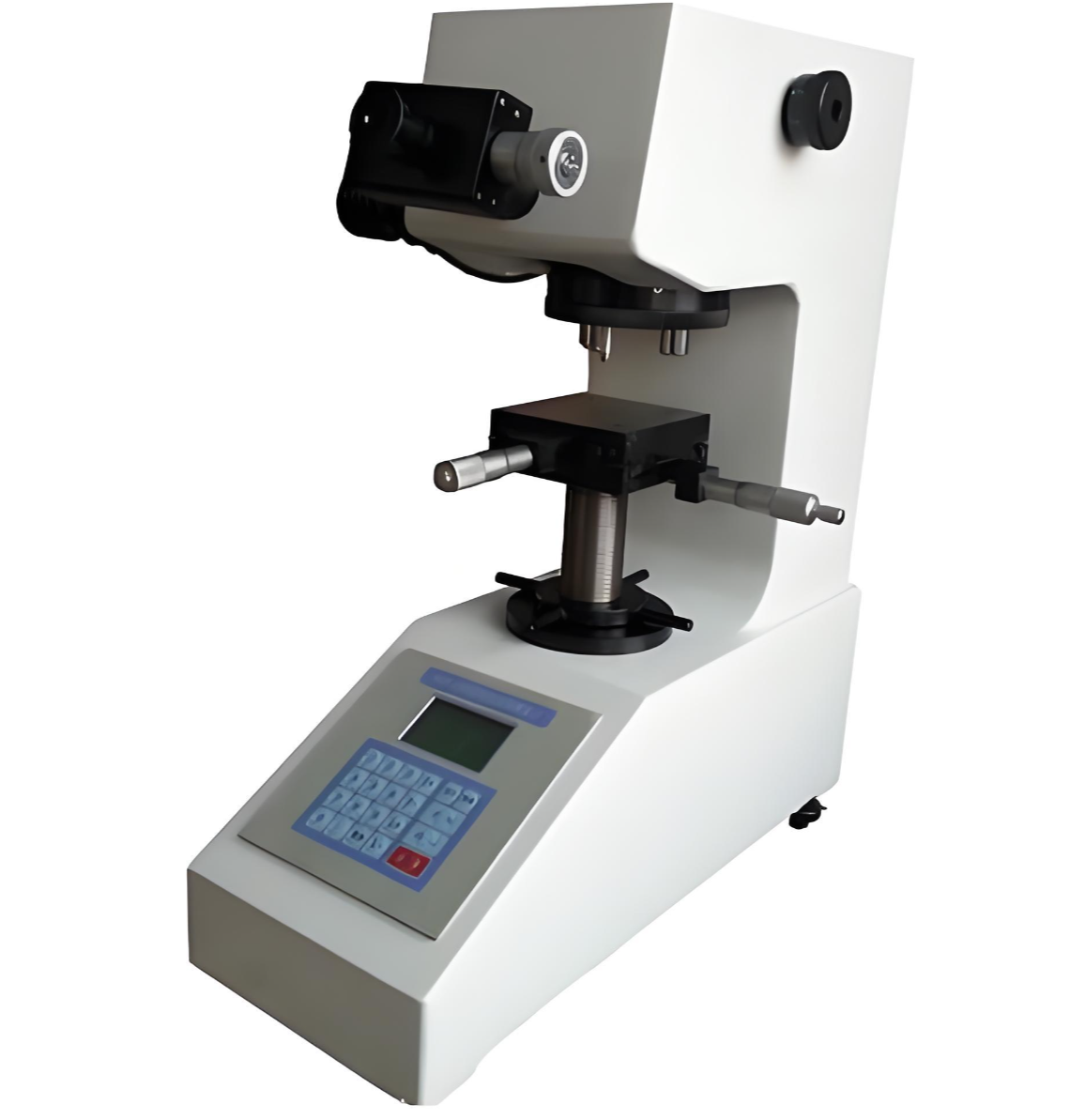
Supporting Failure Analysis and Process Optimization for Continuous Improvement
When a microelectronic component fails, identifying the root cause is paramount to prevent recurrence. Microhardness testers are vital tools in the failure analysis (FA) laboratory. They can be used to perform highly localized hardness measurements on a failed part, such as near a crack initiation point or a fractured bond pad. A deviation in hardness from the specification might indicate issues like improper annealing, contamination, or overtempering, which could have led to embrittlement or softening. This objective data provides crucial clues for pinpointing the stage in the manufacturing process where the defect was introduced. Furthermore, microhardness testing is used proactively for process development and optimization. For instance, when developing a new soldering technique or a thinner coating, engineers can use microhardness data to compare different parameters and select the recipe that yields the optimal balance of hardness, ductility, and adhesion, thereby driving innovation and continuous improvement in manufacturing quality.
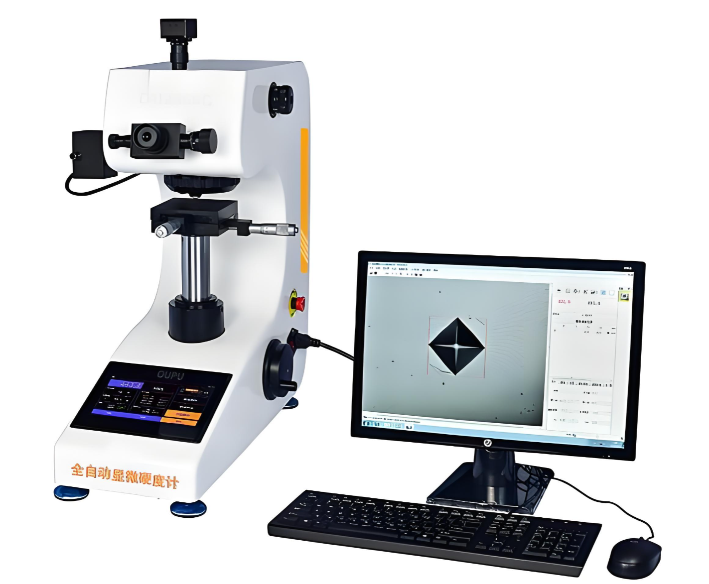
In the high-stakes world of semiconductors and electronics, where failure is not an option, microhardness testers provide the critical, data-driven insights needed to guarantee material integrity, validate complex processes, and solve elusive failures. They are not merely testing instruments but essential enablers of quality, reliability, and miniaturization, ensuring that the tiny components powering our modern world meet the most stringent performance standards.