


Reducing Rejection Rates in Electronics with X-Ray Inspection
Reducing Rejection Rates in Electronics with X-Ray Inspection
Unveiling Hidden Defects: The Power of Non-Destructive Testing
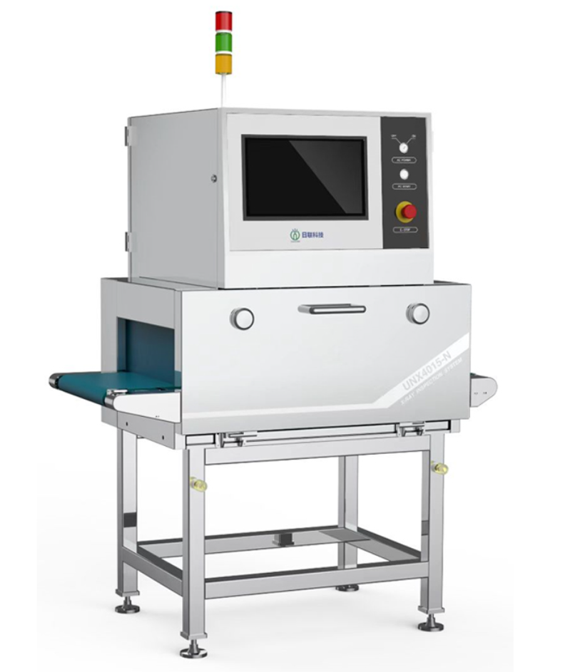
In the highly competitive electronics manufacturing industry, minimizing rejection rates is paramount to profitability and brand reputation. Traditional inspection methods, such as visual checks or functional testing, are limited to surface-level or post-assembly verification. This is where X-ray inspection emerges as a game-changing technology. By utilizing penetrating X-rays, inspection systems like those offered by Skyline International can peer directly into the internal structure of components and assemblies without causing any damage. This non-destructive testing (NDT) capability allows manufacturers to identify critical, hidden defects that are otherwise invisible. Key flaws detectable include solder joint voids, cracks within Ball Grid Array (BGA) packages, misaligned components, and broken wire bonds. By catching these issues early in the production process, manufacturers can prevent faulty products from proceeding down the line, significantly reducing costly final-stage rejections and rework.
From PCBAs to Semiconductors: Comprehensive Quality Assurance
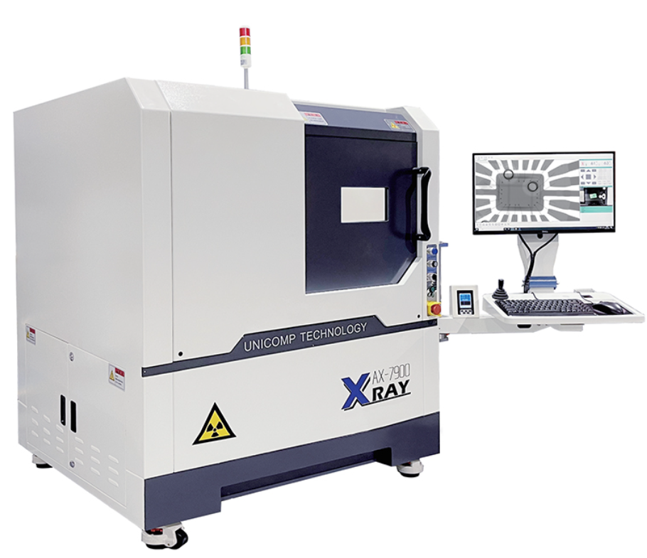
The application of X-ray inspection spans the entire electronics value chain, providing comprehensive quality assurance. For Printed Circuit Board Assemblies (PCBAs), it is indispensable for verifying the integrity of complex solder connections, especially for high-density components like BGAs and Quad Flat No-lead (QFN) packages where connections are hidden beneath the chip. In semiconductor manufacturing, X-ray systems are critical for inspecting die attachments, wire bond quality, and detecting contamination or delamination within encapsulated chips. Furthermore, for emerging technologies such as electric vehicle power electronics and advanced packaging (e.g., 2.5D/3D IC integration), X-ray inspection is the only reliable method to ensure structural soundness. Automated X-ray systems can be integrated into production lines for 100% inspection of critical components or used for statistical process control, providing invaluable data to optimize soldering profiles and assembly parameters, thereby addressing the root causes of defects.
The ROI of Precision: Cost Savings and Brand Protection
Implementing X-ray inspection is a strategic investment that delivers a substantial return on investment by transforming quality control from a cost center into a value generator. The direct cost savings are evident through the drastic reduction in scrap and rework. By identifying defects at the source, manufacturers save on the material, labor, and time costs associated with repairing finished products or discarding them entirely. Beyond direct savings, the long-term benefits are even more significant. Preventing defective products from reaching customers safeguards the company's reputation, minimizes warranty claims, and avoids potentially catastrophic field failures, which is especially critical in automotive, medical, or aerospace applications. The detailed imagery and data generated by X-ray systems also serve as objective evidence for quality audits and supplier evaluations, fostering a culture of continuous improvement and strengthening the entire supply chain's reliability.
An Indispensable Tool for Modern Electronics Manufacturing
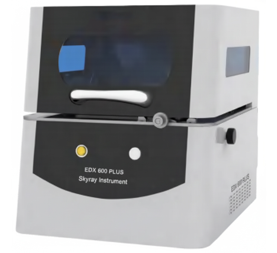
In conclusion, X-ray inspection is no longer a luxury but an indispensable tool for achieving near-zero defect rates in modern electronics manufacturing. Its unparalleled ability to non-destructively reveal hidden flaws empowers manufacturers to move from reactive problem-solving to proactive quality assurance. By integrating advanced X-ray solutions from providers like Skyline International, companies can not only achieve dramatic reductions in rejection rates and associated costs but also build a foundation of quality that enhances product reliability, ensures customer satisfaction, and secures a competitive edge in the demanding global market.