


Precision Inspection Workflow for Semiconductor Manufacturing
Precision Inspection Workflow for Semiconductor Manufacturing
Incoming Material and Front-End Inspection
The semiconductor manufacturing process is a pinnacle of modern precision engineering, where nanometer-scale tolerances dictate the performance and yield of the final chip. A rigorous, multi-stage precision inspection workflow is indispensable to ensure this reliability. The journey begins with the inspection of incoming materials, primarily the silicon wafers themselves. At this stage, tools like laser scanning confocal microscopes and surface roughness testers are critical for characterizing wafer flatness, nanotopography, and surface quality. Any defect here can propagate through all subsequent processes. Following wafer fabrication, which includes photolithography, etching, and doping, front-end inspection becomes paramount. This involves using high-resolution optical measurement projectors and automatic vision inspection systems to measure critical dimensions (CDs) of transistor gates and other patterned features. Suzhou Xinhe Measurement Instrument Co., Ltd. supplies advanced microscopes and measurement systems that enable manufacturers to detect minute defects, verify line widths, and ensure that the intricate patterns etched onto the wafer conform to the exacting design specifications, laying a flawless foundation for the device's functionality.
Ensuring Structural Integrity and Interconnect Reliability in Back-End Processes
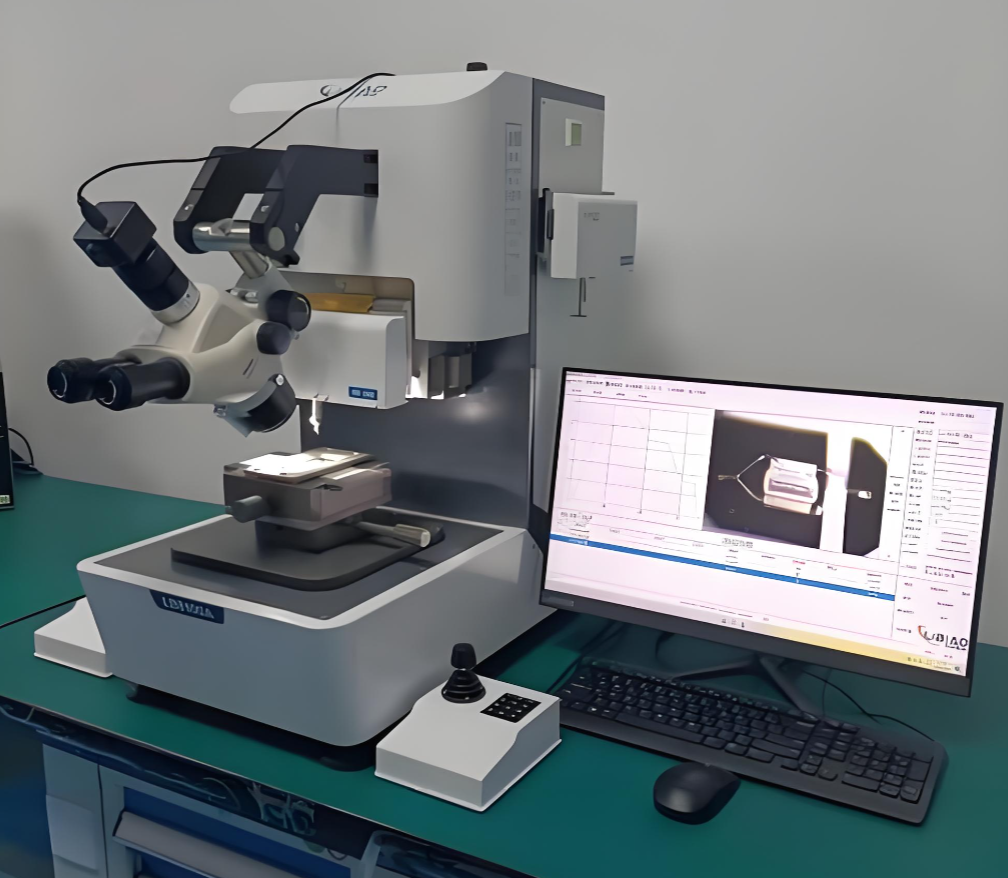
Once the individual devices on the wafer are created, the focus shifts to the back-end processes that interconnect them and prepare the chip for packaging. This phase introduces new inspection challenges related to structural integrity and material properties. Scanning Acoustic Microscopy (C-SAM / SAT) is a vital non-destructive technique used to detect delamination, voids, and cracks within the chip's internal structure, such as in the die-attach layer or underfill material. Similarly, microhardness testers, including Vickers and Knoop scales, are employed to measure the hardness of thin films and various substrate materials, which is a proxy for their mechanical stability and resistance to stress-induced failures. For analyzing material composition and identifying contaminants, X-ray fluorescence (XRF) analyzers and scanning electron microscopes (SEM) become essential. Skyline International provides these sophisticated analytical tools to manufacturers in Vietnam, enabling them to perform root cause analysis on failures and validate the quality of metallization layers and solder bumps, ensuring robust electrical connections and long-term device reliability.
Final Verification, Cleanliness, and Packaging Inspection
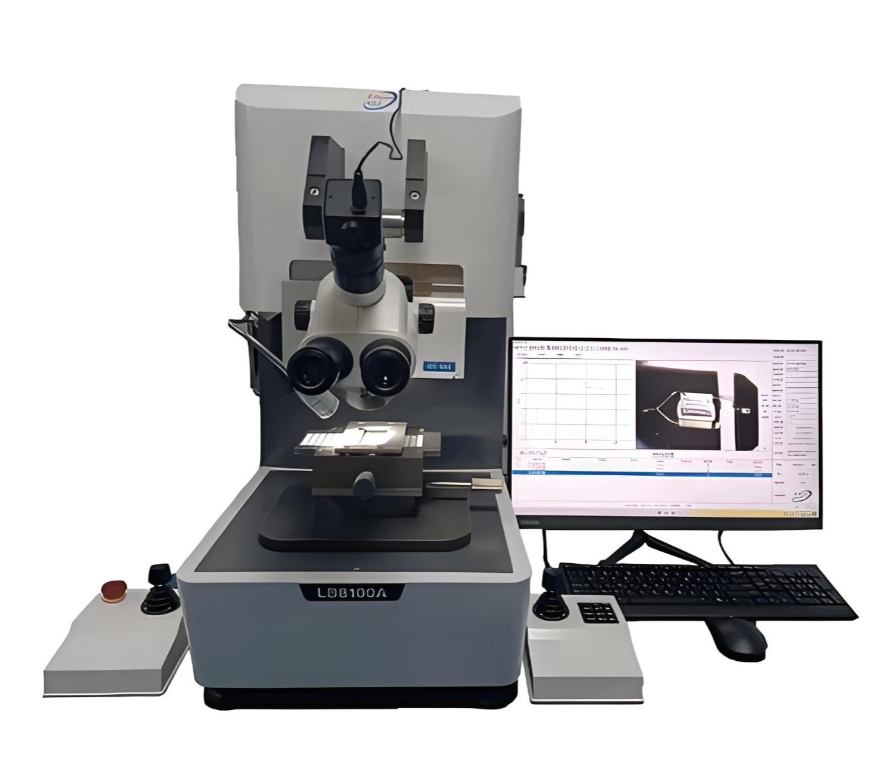
The final stage of the workflow involves verifying the packaged chip's quality and readiness for the end application. Packaging inspection ensures that the external dimensions, lead flatness, and coplanarity meet the required standards, often using video measurement systems and high-precision calipers. Furthermore, the growing demand for automotive and medical-grade semiconductors places extreme importance on cleanliness testing. Automotive parts cleanliness testing systems are used to analyze particulate contamination on the chip surface, as even microscopic particles can cause catastrophic failures in sensitive applications. Finally, functional tests are complemented by mechanical verification. Tools like bond pull testers assess the strength of wire bonds, while thermal cycling chambers and environmental test chambers subject the finished devices to accelerated life testing, simulating years of operation in a short time to guarantee their durability. Suzhou Xinhe's comprehensive portfolio supports this entire final verification phase, providing the metrology backbone needed to certify that every semiconductor device leaving the production line is not only functional but also reliable enough for its intended mission.
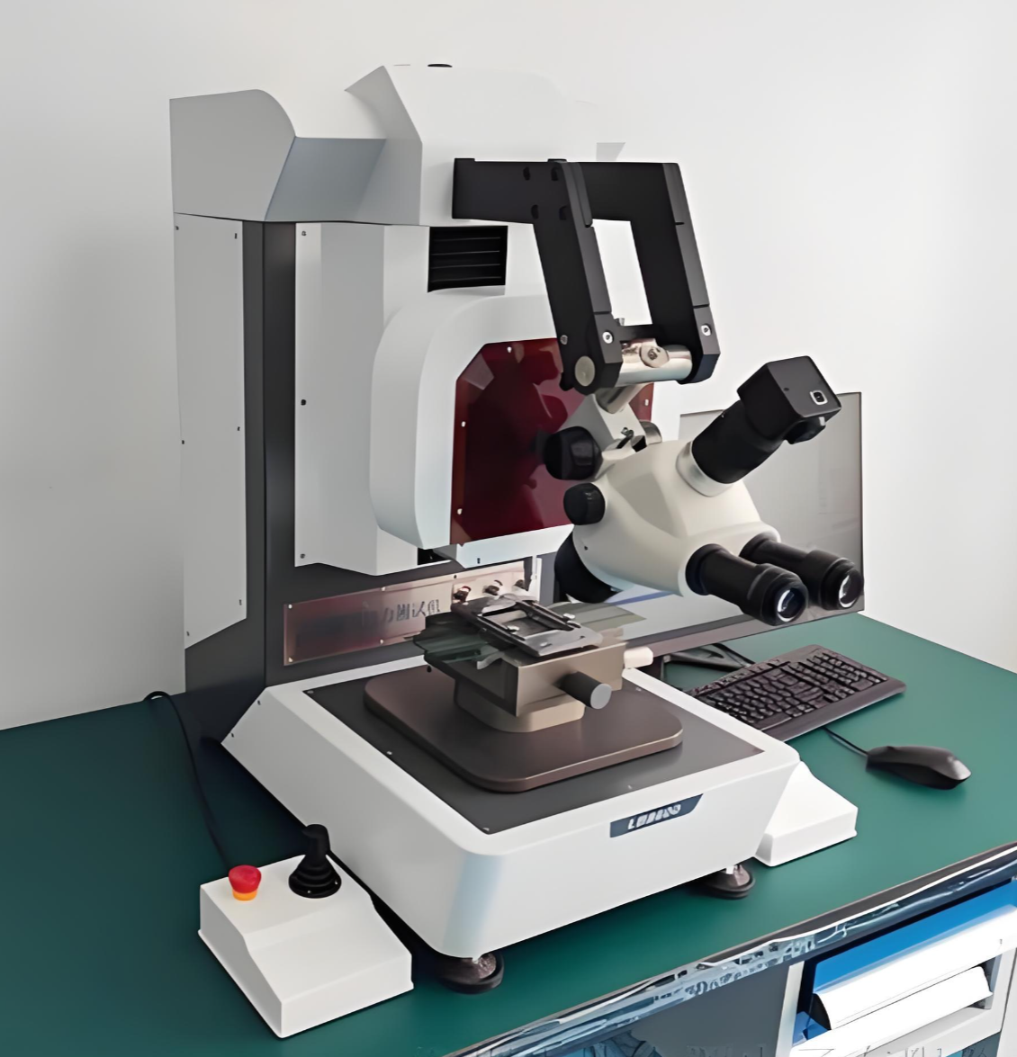
In conclusion, the precision inspection workflow in semiconductor manufacturing is a complex, interconnected chain where each link—from wafer inspection to final package testing—is critical. It relies on a sophisticated arsenal of metrology instruments to visualize, measure, and analyze features and properties at micro and nano scales. Suzhou Xinhe Measurement Instrument Co., Ltd. and its partner Skyline International are positioned as key enablers in this high-stakes industry. By providing the essential tools for every step of this workflow, they empower semiconductor manufacturers to achieve the extraordinary levels of quality, reliability, and yield demanded by today's technology-driven world.