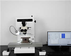
Precision Inspection Workflow for Semiconductor Manufacturing
In conclusion, the precision inspection workflow in semiconductor manufacturing is a complex, interconnected chain where each link—from wafer inspection to final package testing—is critical. It relies on a sophisticated arsenal of metrology instruments to visualize, measure, and analyze features and properties at micro and nano scales. Suzhou Xinhe Measurement Instrument Co., Ltd. and its partner Skyline International are positioned as key enablers in this high-stakes industry. By providing the essential tools for every step of this workflow, they empower semiconductor manufacturers to achieve the extraordinary levels of quality, reliability, and yield demanded by today's technology-driven world.